Thursday, December 26, 2013
Stereo Preamplifier With Bass Boost
High Quality, simple design, DC 20v to 30v supply
This preamplifier was designed to cope with CD players, tuners, tape recorders etc., providing an ac voltage gain of 4, in order to drive less sensitive power amplifiers. As modern Hi-Fi home equipment is frequently fitted with small loudspeaker cabinets, the bass frequency range is rather sacrificed. This circuit features also a bass-boost, in order to overcome this problem. You can use a variable resistor to set the bass-boost from 0 to a maximum of +16dB @ 30Hz. If a fixed, maximum boost value is needed, the variable resistor can be omitted and substituted by a switch.
Stereo Preamplifier With Bass Boost Circuit diagram:

P1 = 10K
P2 = 100K
R1 = 100K
R2 = 100K
R3 = 15K
R4 = 10K
R5 = 22K
R6 = 15K
R7 = 1K
R8 = 470R
C1 = 2.2uF-25v
C2 = 2.2uF-25v
C3 = 470uF-35v
C4 = 1uF-35V
C5 = 2.2uF-25v
C6 = 47nF-63v
C7 = 22uF-25v
IC1 = TL072, Opamp
SW1 = DPST Switch
Notes:
- Schematic shows left channel only, but R1, R2, R3 and C1, C2, C3 are common to both channels.
- For stereo operation P1, P2 (or SW1), R4, R5, R6, R7, R8 and C4, C5, C6, C7 must be doubled.
- Numbers in parentheses show IC1 right channel pin connections.
- A log type for P2 ensures a more linear regulation of bass-boost.
- Needing a simple boost-in boost-out operation, P2 must be omitted and SW1 added as shown in the diagram.
- For stereo operation SW1 must be a DPST type.
- Please note that, using SW1, the boost is on when the switch is open, and off when the switch is closed.
Source : http://www.ecircuitslab.com/2011/06/stereo-preamplifier-with-bass-boost.html
Tuesday, December 24, 2013
mobile phone jammer can be installed in the ceiling in the hall
The antenna of mobile phone jammer should be perpendicular to the ground
Introduced Vodafone (LSE: VOD NYSE: VOD) (Vodafone) is a multinational mobile phone operators. Newbury (Newbury), headquartered in Berkshire County, England and Dusseldorf, Germany. Is currently one of the worlds largest mobile telecommunications network company, have investments in 27 countries around the world. Do co-operate with the local mobile phone operators in 14 countries, the mobile phone network of associates. As of December 31, 2004, Vodafone has about 151.8 million users in the world. Vodafone Vodafone Group as the name listed on the London Stock Exchange (code VOD.L) and the NYSE (symbol VOD). mobile phone jammer can be installed in the ceiling in the hall.
AT & T will be the "information superhighway" the plan participants. Will achieve the ideal of mankind - the establishment of a global information service system, so that people anywhere convenient to contact, the sharing of information resources to meet the advent of the information society. Germany Vodafone vodafone Vodafone (in vodafone KK) is the worlds largest mobile communications operator, and its network covering 26 countries, and to provide network services in 31 countries and their partners, over 179 million users worldwide. Vodafone has the worlds most comprehensive enterprise information management systems and customer service systems, service delivery, increase customer has a strong advantage in creating value. Here will show the bulk shielding of mobile phone jammer in a building.
In addition to Spains four stock (Madrid, Barcelona, Bilbao and Valencia), Spain, the telephone companys stock is still in London, Paris, Frankfurt, Tokyo, New York, Sao Paulo, Limas stock market and London the SEAQ International stock trading system to trade. In order to remain invincible in the fierce competition in international telecommunications market, the telephone company in Spain organized a series of international business lines, operated by an independent company. Such a flexible management style is conducive to take measures according to their characteristics, can also enhance the financial strength through joint ventures. Not long ago, the Spanish telephone company into the Internet field, by the same company responsible for production and sales operations. Shielding effect of mobile phone jammer is dependent on room size.
Meanwhile, Cisco Systems, Inc. is building the backbone of the Internet, more than 80 percent of the Internet backbone routers is Cisco Systems, the companys products. Texas Instruments (TI) - Texas Instruments Incorporated is a global semiconductor company, is the world leader in digital signal processing and analog technologies and suppliers, the semiconductor engines of the Internet age. The worlds first integrated circuit (IC) was invented by TI engineer Jack Kilby. The company is headquartered in Dallas, Texas, its business, including semiconductor, industrial, electronic materials, educational products. Companies in over 25 countries worldwide and has manufacturing or sales organization. In this method, there is no need to install mobile phone jammer on the outer wall of every floor.
More...
Introduced Vodafone (LSE: VOD NYSE: VOD) (Vodafone) is a multinational mobile phone operators. Newbury (Newbury), headquartered in Berkshire County, England and Dusseldorf, Germany. Is currently one of the worlds largest mobile telecommunications network company, have investments in 27 countries around the world. Do co-operate with the local mobile phone operators in 14 countries, the mobile phone network of associates. As of December 31, 2004, Vodafone has about 151.8 million users in the world. Vodafone Vodafone Group as the name listed on the London Stock Exchange (code VOD.L) and the NYSE (symbol VOD). mobile phone jammer can be installed in the ceiling in the hall.
AT & T will be the "information superhighway" the plan participants. Will achieve the ideal of mankind - the establishment of a global information service system, so that people anywhere convenient to contact, the sharing of information resources to meet the advent of the information society. Germany Vodafone vodafone Vodafone (in vodafone KK) is the worlds largest mobile communications operator, and its network covering 26 countries, and to provide network services in 31 countries and their partners, over 179 million users worldwide. Vodafone has the worlds most comprehensive enterprise information management systems and customer service systems, service delivery, increase customer has a strong advantage in creating value. Here will show the bulk shielding of mobile phone jammer in a building.
In addition to Spains four stock (Madrid, Barcelona, Bilbao and Valencia), Spain, the telephone companys stock is still in London, Paris, Frankfurt, Tokyo, New York, Sao Paulo, Limas stock market and London the SEAQ International stock trading system to trade. In order to remain invincible in the fierce competition in international telecommunications market, the telephone company in Spain organized a series of international business lines, operated by an independent company. Such a flexible management style is conducive to take measures according to their characteristics, can also enhance the financial strength through joint ventures. Not long ago, the Spanish telephone company into the Internet field, by the same company responsible for production and sales operations. Shielding effect of mobile phone jammer is dependent on room size.
Meanwhile, Cisco Systems, Inc. is building the backbone of the Internet, more than 80 percent of the Internet backbone routers is Cisco Systems, the companys products. Texas Instruments (TI) - Texas Instruments Incorporated is a global semiconductor company, is the world leader in digital signal processing and analog technologies and suppliers, the semiconductor engines of the Internet age. The worlds first integrated circuit (IC) was invented by TI engineer Jack Kilby. The company is headquartered in Dallas, Texas, its business, including semiconductor, industrial, electronic materials, educational products. Companies in over 25 countries worldwide and has manufacturing or sales organization. In this method, there is no need to install mobile phone jammer on the outer wall of every floor.
Sunday, December 22, 2013
Electronic Water Alarm
Aburst water-supply hose of the washing machine, a bathroom tap that you forgot to close, or a broken aquarium wall may turn your house into a pond. You can avoid this mess by using an electronic water alarm that warns you of the water leakage as soon as possible. The acoustic water alarm circuit presented here takes advantage of the fact that the tap water is always slightly contaminated (or has salts and minerals) and thus conducts electricity to a certain extent.
It is built around IC LMC555 (IC1), which is a CMOS version of the bipolar 555 timer chip. IC1 is followed by a complementary pair of emitter followers (T1 and T2) to drive a standard 8-ohm speaker (LS1). Power is supplied by a compact 9V PP3 battery. Power is applied when power switch S1 is closed. The reset input (pin 4) of IC1 is held low by resistor R1 (2.2-kilo-ohm).
The astable oscillator wired around IC1 is in disabled mode. When probes P1 and P2 become wet, these conduct to reverse the state of IC1’s reset terminal. As a result, the astable multivibrator starts oscillating at a frequency determined by resistor R2 and capacitor C3. The output of IC1 drives the complementary pair of transistors T1 and T2.
Although this combination causes significant crossover distortion, it doesn’t have any adverse effect on the square-wave audio signal processing. A 10-kilo-ohm potentiometer (VRI) is inserted between output pin 3 of IC1 and the bases of transistors T1 and T2 for volume control. The probes can be made using two suitable copper needles or small pieces of circuit board with the copper surface coated with solder.
Fit these at the lowest point where water will accumulate. After construction, place the alarm circuit well away from the point of possible leakage. Use a pair of thin twisted flexible wires to connect the probes to the circuit. Capacitor C1 connected across IC1 input (pin 4 and GND) keeps the alarm circuit from responding to stray electrostatic fields.
Similarly, twisting the wires together makes the relatively long connection between the probes and the circuit less sensitive to false alarms due to external electromagnetic interference. Finally, if you want to lower the probe sensitivity, reduce the value of grounding resistor R1.
More...
It is built around IC LMC555 (IC1), which is a CMOS version of the bipolar 555 timer chip. IC1 is followed by a complementary pair of emitter followers (T1 and T2) to drive a standard 8-ohm speaker (LS1). Power is supplied by a compact 9V PP3 battery. Power is applied when power switch S1 is closed. The reset input (pin 4) of IC1 is held low by resistor R1 (2.2-kilo-ohm).
The astable oscillator wired around IC1 is in disabled mode. When probes P1 and P2 become wet, these conduct to reverse the state of IC1’s reset terminal. As a result, the astable multivibrator starts oscillating at a frequency determined by resistor R2 and capacitor C3. The output of IC1 drives the complementary pair of transistors T1 and T2.
 |
| Electronic Water Alarm Circuit Diagram |
Fit these at the lowest point where water will accumulate. After construction, place the alarm circuit well away from the point of possible leakage. Use a pair of thin twisted flexible wires to connect the probes to the circuit. Capacitor C1 connected across IC1 input (pin 4 and GND) keeps the alarm circuit from responding to stray electrostatic fields.
Similarly, twisting the wires together makes the relatively long connection between the probes and the circuit less sensitive to false alarms due to external electromagnetic interference. Finally, if you want to lower the probe sensitivity, reduce the value of grounding resistor R1.
Friday, December 20, 2013
Cell Phone Jammers has no radiation towards the human body
Cell Phone Jammers has no radiation towards the human body.
Although almost all manufacturers have in recent years tend to use lithium-ion battery, but the worlds major mobile phone manufacturers the choice of battery or have their own characteristics and habits, such as once in the same historical period: Nokia: The Ni- MH (nickel-metal hydride) battery, LiB (liquid lithium-ion) batteries, not the use of LiP (polymer lithium-ion) batteries. Ericsson: The Ni-MH battery, LiB battery, LiP batteries. Motorola: The Ni-MH battery, LiB battery, did not use LiP batteries. Not difficult to find, from the earliest use of mobile phones LiP polymer lithium-ion batteries on this matter, Ericsson reflect the true nature of their cell phone technology pioneer. According to the information I find that, at present polymer lithium-ion battery factory in Japan SONY, Panasonic, GS, several companies, produced in 2000 reached 21 million, of which 50% of Ericsson mobile phone support.
This environment is very noisy radio environments, it is even more obvious advantages. Another advantage of Bluetooth technology is that it applies globally consistent set of frequencies, which eliminates the "border" barriers, while in the field of cellular mobile phones, this obstacle has been plagued users for many years. In addition, ISM band radio system for all the bands are open, so use one of these bands will encounter unpredictable sources of interference. For example, some appliances, cordless phones, car room door openers, microwave ovens, etc., are likely to be interference. The inspection report of Cell Phone Jammers needs the signature of the director of Cell Phone Jammers workshop.
To this end, the Bluetooth technology, especially designed to quickly identify and frequency hopping scheme to ensure that the link stability. Band frequency hopping is to be divided into a number of hopping channels (hop channel), in a single connection, the radio transceiver according to a certain code sequence constantly jump from one channel to another channel, only the sender and receiver to communicate is based on the law , and other interference can not be carried out by the same laws of interference; hopping the instantaneous bandwidth is very narrow, but through spread spectrum technology make this expansion into narrowband or broadband multiply, so that interference effects may become very small. Work with other systems compared to the same frequency band, Bluetooth frequency hopping faster, shorter packets, which makes Bluetooth technology are more stable than other systems. Chipset mainly refers to the Bluetooth headset Bluetooth chips used in the design of the composition. Bluetooth chip on the market today many manufacturers. Major telecommunications manufacturers have designed in accordance with Bluetooth standards have different chipsets. The factory inspection and acceptance personnel should sign the report of Cell Phone Jammers if Cell Phone Jammers is qualified.
More...
Although almost all manufacturers have in recent years tend to use lithium-ion battery, but the worlds major mobile phone manufacturers the choice of battery or have their own characteristics and habits, such as once in the same historical period: Nokia: The Ni- MH (nickel-metal hydride) battery, LiB (liquid lithium-ion) batteries, not the use of LiP (polymer lithium-ion) batteries. Ericsson: The Ni-MH battery, LiB battery, LiP batteries. Motorola: The Ni-MH battery, LiB battery, did not use LiP batteries. Not difficult to find, from the earliest use of mobile phones LiP polymer lithium-ion batteries on this matter, Ericsson reflect the true nature of their cell phone technology pioneer. According to the information I find that, at present polymer lithium-ion battery factory in Japan SONY, Panasonic, GS, several companies, produced in 2000 reached 21 million, of which 50% of Ericsson mobile phone support.
This environment is very noisy radio environments, it is even more obvious advantages. Another advantage of Bluetooth technology is that it applies globally consistent set of frequencies, which eliminates the "border" barriers, while in the field of cellular mobile phones, this obstacle has been plagued users for many years. In addition, ISM band radio system for all the bands are open, so use one of these bands will encounter unpredictable sources of interference. For example, some appliances, cordless phones, car room door openers, microwave ovens, etc., are likely to be interference. The inspection report of Cell Phone Jammers needs the signature of the director of Cell Phone Jammers workshop.
To this end, the Bluetooth technology, especially designed to quickly identify and frequency hopping scheme to ensure that the link stability. Band frequency hopping is to be divided into a number of hopping channels (hop channel), in a single connection, the radio transceiver according to a certain code sequence constantly jump from one channel to another channel, only the sender and receiver to communicate is based on the law , and other interference can not be carried out by the same laws of interference; hopping the instantaneous bandwidth is very narrow, but through spread spectrum technology make this expansion into narrowband or broadband multiply, so that interference effects may become very small. Work with other systems compared to the same frequency band, Bluetooth frequency hopping faster, shorter packets, which makes Bluetooth technology are more stable than other systems. Chipset mainly refers to the Bluetooth headset Bluetooth chips used in the design of the composition. Bluetooth chip on the market today many manufacturers. Major telecommunications manufacturers have designed in accordance with Bluetooth standards have different chipsets. The factory inspection and acceptance personnel should sign the report of Cell Phone Jammers if Cell Phone Jammers is qualified.
Wednesday, December 18, 2013
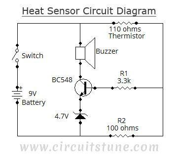
Heat Sensor Circuit Diagram
This simple heat sensor circuit could senses heat from various electronics device like computer, amplifier etc. and generate warning alarm. It could senses heat from environment also, but here I mention “electronics device” because it is being using mostly in electronic device to protect them from overheat.
Circuit diagram of heat sensor:
 |
| Fig-1: Schematic Circuit Diagram Of Heat/Temperature Sensor |
Thermistor, 110 Ohms:
 |
| Fig-2: 110 Ohms Thermistor |
As it is a heat sensor circuit, here a thermistor is used as a heat sensor. It is a thermal measurement device and has a variety of usages including temperature sensor/ heat sensor. The thermistor used in this circuit is a NTC (Negative Temperature Coefficient) type thermistor. When temperature increases, its resistance goes decrease. Therefore, NTC thermistor’s resistances are inverse of temperature.
Circuit Description:
You have seen, in this simple circuit diagram of heat sensor, a few number of components is used including a BC548 transistor, a 110 ohms thermistor etc.- BC548: BC548 is a TO-92 type NPN transistor, as its alternative you can use 2N2222, BC238, BC548, BC168, BC183 etc. they all have almost same characteristic.
- 110 Ohms Thermistor: A 110 Ohms thermistor is used to detecting heat. I have told already about it.
- Buzzer: A buzzer is used with +9V and collector of transistor. When the temperature/ heat exceeds a certain level then it make an alarm.
- 4.7V Zener diode: It is used to limit the emitter current of BC548.
- 9V Battery: A 9V battery is used as a single power source.
- R1, R2: A 3.3K 1/4w resistor is used as R1 and 100 ohms 1/4w as R2.
- Switch: Here in this circuit the switch used is a simple SPST switch. You can either use the switch or not, choice is yours. It is not mandatory.
Tuesday, October 8, 2013
AF Amplifier With Digital Volume Control Based On TDA8551
The Philips Semiconductors TDA8551 is a small audio amplifier with an integrated volume control. When operated from +5 V, it delivers a nominal output power of more than one watt into 8 ohms. It can also be used over a supply voltage range of +2.7 to +5.5 V, with correspondingly reduced output power. The output volume can be adjusted from –60 dB to +20 dB in 64 steps, using a set of up and down push-buttons. The shared UP/DOWN input for the up and down switches has three states. If it is ‘floating’, which means that both of the switches are open, the volume remains unchanged. A pulse to earth decreases the volume by 1.25 dB, while a positive pulse increases the volume by 1.25 dB.
 When the power is switched on, the internal counter takes on the –20 dB setting. An additional input (MODE) allows the amplifier to be switched from the operating state to the mute or standby state. If this input is held at the earth level, the amplifier is operational. If +5 V is applied to this pin, the TDA8551 enters the Standby mode, in which the current consumption drops from the typical operational level of 6mA to less than 10µA. Finally, the MODE input can be used as a mute input by applying a voltage of 1 t0 3.6 V to this input. This voltage can be provided by a connection to the SCR pin, which lies at half of the operating voltage and to which a filter capacitor is connected.
 The loudspeaker is connected in a floating configuration between the two outputs of the bridge amplifier in the TDA8551. This provides the desired output power level, in spite of the low supply voltage. For headphone applications, which do not need as much output power, you can connect the headphone between earth and one of the outputs, via an electrolytic coupling capacitor. You can make a stereo headphone amplifier in this way, using two TDS8551 ICs. The TDA8551 is housed in a DIP8 package. The SMD version is the TDA8551T, in an SO8 package.
More...
 When the power is switched on, the internal counter takes on the –20 dB setting. An additional input (MODE) allows the amplifier to be switched from the operating state to the mute or standby state. If this input is held at the earth level, the amplifier is operational. If +5 V is applied to this pin, the TDA8551 enters the Standby mode, in which the current consumption drops from the typical operational level of 6mA to less than 10µA. Finally, the MODE input can be used as a mute input by applying a voltage of 1 t0 3.6 V to this input. This voltage can be provided by a connection to the SCR pin, which lies at half of the operating voltage and to which a filter capacitor is connected.
 The loudspeaker is connected in a floating configuration between the two outputs of the bridge amplifier in the TDA8551. This provides the desired output power level, in spite of the low supply voltage. For headphone applications, which do not need as much output power, you can connect the headphone between earth and one of the outputs, via an electrolytic coupling capacitor. You can make a stereo headphone amplifier in this way, using two TDS8551 ICs. The TDA8551 is housed in a DIP8 package. The SMD version is the TDA8551T, in an SO8 package.
Sunday, October 6, 2013
UPS For Cordless Telephones
Cordless telephones are very popular nowadays. But they have a major drawback, i.e. they cannot be operated during power failure. Therefore usually another ordinary telephone is connected in parallel to the cordless telephone. This results in lack of secrecy. UPS is a permanent solution to this problem. Since the UPS is meant only for the cordless telephone, its output power is limited to around 1.5W. This is sufficient to operate most cordless telephones. as these employ only small capacity adapters (usually 9V/12V, 500mA), to enable the operation of the circuit and to charge the battery present in the handset. The UPS presently designed is of online type. Here the inverter is ‘on’ throughout, irrespective of the presence of the AC mains.
When the AC mains is present, the same is converted into DC and fed to the inverter. A part of the mains rectified output is used to charge the battery. When the mains power fails, the DC supply to the inverter is from the battery and from this is obtained AC at the inverter output. This is shown in fig.1. The circuit wired around IC CD4047 is an astable multivibrator operating at a frequency of 50 Hz. The Q and Q outputs of this multivibrator directly drive power MOSFETS IRF540. The configuration used is push-pull type. The inverter output is filtered and the spikes are reduced using MOV (metal oxide varistor). The inverter transformer used is an ordinary 9V-0-9V, 1.5A mains transformer readily available in the market.
 Two LEDS (D6 and D7) indicate the presence of mains/battery. The mains supply (when present) is stepped down, rectified and filtered using diodes D1 through D4 and capacitor C1. A part of this supply is also used to charge the battery. In place of a single 12V, 4Ah battery, one may use two 6V, 4Ah batteries (SUNCA or any other suitable brand). The circuit can be easily assembled on a general-purpose PCB and placed inside a metal box. The two transformers may be mounted on the chassis of the box. Also, the two batteries can be mounted in the box using supporting clamps. The front and back panel designs are shown in the Fig. 3. The same circuit can deliver up to 100W, provided the inverter transformer and charging transformer are replaced with higher current rating transformers, so that the system can be used for some other applications as well.
More...
When the AC mains is present, the same is converted into DC and fed to the inverter. A part of the mains rectified output is used to charge the battery. When the mains power fails, the DC supply to the inverter is from the battery and from this is obtained AC at the inverter output. This is shown in fig.1. The circuit wired around IC CD4047 is an astable multivibrator operating at a frequency of 50 Hz. The Q and Q outputs of this multivibrator directly drive power MOSFETS IRF540. The configuration used is push-pull type. The inverter output is filtered and the spikes are reduced using MOV (metal oxide varistor). The inverter transformer used is an ordinary 9V-0-9V, 1.5A mains transformer readily available in the market.
 Two LEDS (D6 and D7) indicate the presence of mains/battery. The mains supply (when present) is stepped down, rectified and filtered using diodes D1 through D4 and capacitor C1. A part of this supply is also used to charge the battery. In place of a single 12V, 4Ah battery, one may use two 6V, 4Ah batteries (SUNCA or any other suitable brand). The circuit can be easily assembled on a general-purpose PCB and placed inside a metal box. The two transformers may be mounted on the chassis of the box. Also, the two batteries can be mounted in the box using supporting clamps. The front and back panel designs are shown in the Fig. 3. The same circuit can deliver up to 100W, provided the inverter transformer and charging transformer are replaced with higher current rating transformers, so that the system can be used for some other applications as well.
Subscribe to:
Posts (Atom)