Thursday, December 26, 2013
Stereo Preamplifier With Bass Boost
High Quality, simple design, DC 20v to 30v supply
This preamplifier was designed to cope with CD players, tuners, tape recorders etc., providing an ac voltage gain of 4, in order to drive less sensitive power amplifiers. As modern Hi-Fi home equipment is frequently fitted with small loudspeaker cabinets, the bass frequency range is rather sacrificed. This circuit features also a bass-boost, in order to overcome this problem. You can use a variable resistor to set the bass-boost from 0 to a maximum of +16dB @ 30Hz. If a fixed, maximum boost value is needed, the variable resistor can be omitted and substituted by a switch.
Stereo Preamplifier With Bass Boost Circuit diagram:

P1 = 10K
P2 = 100K
R1 = 100K
R2 = 100K
R3 = 15K
R4 = 10K
R5 = 22K
R6 = 15K
R7 = 1K
R8 = 470R
C1 = 2.2uF-25v
C2 = 2.2uF-25v
C3 = 470uF-35v
C4 = 1uF-35V
C5 = 2.2uF-25v
C6 = 47nF-63v
C7 = 22uF-25v
IC1 = TL072, Opamp
SW1 = DPST Switch
Notes:
- Schematic shows left channel only, but R1, R2, R3 and C1, C2, C3 are common to both channels.
- For stereo operation P1, P2 (or SW1), R4, R5, R6, R7, R8 and C4, C5, C6, C7 must be doubled.
- Numbers in parentheses show IC1 right channel pin connections.
- A log type for P2 ensures a more linear regulation of bass-boost.
- Needing a simple boost-in boost-out operation, P2 must be omitted and SW1 added as shown in the diagram.
- For stereo operation SW1 must be a DPST type.
- Please note that, using SW1, the boost is on when the switch is open, and off when the switch is closed.
Source : http://www.ecircuitslab.com/2011/06/stereo-preamplifier-with-bass-boost.html
Tuesday, December 24, 2013
mobile phone jammer can be installed in the ceiling in the hall
The antenna of mobile phone jammer should be perpendicular to the ground
Introduced Vodafone (LSE: VOD NYSE: VOD) (Vodafone) is a multinational mobile phone operators. Newbury (Newbury), headquartered in Berkshire County, England and Dusseldorf, Germany. Is currently one of the worlds largest mobile telecommunications network company, have investments in 27 countries around the world. Do co-operate with the local mobile phone operators in 14 countries, the mobile phone network of associates. As of December 31, 2004, Vodafone has about 151.8 million users in the world. Vodafone Vodafone Group as the name listed on the London Stock Exchange (code VOD.L) and the NYSE (symbol VOD). mobile phone jammer can be installed in the ceiling in the hall.
AT & T will be the "information superhighway" the plan participants. Will achieve the ideal of mankind - the establishment of a global information service system, so that people anywhere convenient to contact, the sharing of information resources to meet the advent of the information society. Germany Vodafone vodafone Vodafone (in vodafone KK) is the worlds largest mobile communications operator, and its network covering 26 countries, and to provide network services in 31 countries and their partners, over 179 million users worldwide. Vodafone has the worlds most comprehensive enterprise information management systems and customer service systems, service delivery, increase customer has a strong advantage in creating value. Here will show the bulk shielding of mobile phone jammer in a building.
In addition to Spains four stock (Madrid, Barcelona, Bilbao and Valencia), Spain, the telephone companys stock is still in London, Paris, Frankfurt, Tokyo, New York, Sao Paulo, Limas stock market and London the SEAQ International stock trading system to trade. In order to remain invincible in the fierce competition in international telecommunications market, the telephone company in Spain organized a series of international business lines, operated by an independent company. Such a flexible management style is conducive to take measures according to their characteristics, can also enhance the financial strength through joint ventures. Not long ago, the Spanish telephone company into the Internet field, by the same company responsible for production and sales operations. Shielding effect of mobile phone jammer is dependent on room size.
Meanwhile, Cisco Systems, Inc. is building the backbone of the Internet, more than 80 percent of the Internet backbone routers is Cisco Systems, the companys products. Texas Instruments (TI) - Texas Instruments Incorporated is a global semiconductor company, is the world leader in digital signal processing and analog technologies and suppliers, the semiconductor engines of the Internet age. The worlds first integrated circuit (IC) was invented by TI engineer Jack Kilby. The company is headquartered in Dallas, Texas, its business, including semiconductor, industrial, electronic materials, educational products. Companies in over 25 countries worldwide and has manufacturing or sales organization. In this method, there is no need to install mobile phone jammer on the outer wall of every floor.
More...
Introduced Vodafone (LSE: VOD NYSE: VOD) (Vodafone) is a multinational mobile phone operators. Newbury (Newbury), headquartered in Berkshire County, England and Dusseldorf, Germany. Is currently one of the worlds largest mobile telecommunications network company, have investments in 27 countries around the world. Do co-operate with the local mobile phone operators in 14 countries, the mobile phone network of associates. As of December 31, 2004, Vodafone has about 151.8 million users in the world. Vodafone Vodafone Group as the name listed on the London Stock Exchange (code VOD.L) and the NYSE (symbol VOD). mobile phone jammer can be installed in the ceiling in the hall.
AT & T will be the "information superhighway" the plan participants. Will achieve the ideal of mankind - the establishment of a global information service system, so that people anywhere convenient to contact, the sharing of information resources to meet the advent of the information society. Germany Vodafone vodafone Vodafone (in vodafone KK) is the worlds largest mobile communications operator, and its network covering 26 countries, and to provide network services in 31 countries and their partners, over 179 million users worldwide. Vodafone has the worlds most comprehensive enterprise information management systems and customer service systems, service delivery, increase customer has a strong advantage in creating value. Here will show the bulk shielding of mobile phone jammer in a building.
In addition to Spains four stock (Madrid, Barcelona, Bilbao and Valencia), Spain, the telephone companys stock is still in London, Paris, Frankfurt, Tokyo, New York, Sao Paulo, Limas stock market and London the SEAQ International stock trading system to trade. In order to remain invincible in the fierce competition in international telecommunications market, the telephone company in Spain organized a series of international business lines, operated by an independent company. Such a flexible management style is conducive to take measures according to their characteristics, can also enhance the financial strength through joint ventures. Not long ago, the Spanish telephone company into the Internet field, by the same company responsible for production and sales operations. Shielding effect of mobile phone jammer is dependent on room size.
Meanwhile, Cisco Systems, Inc. is building the backbone of the Internet, more than 80 percent of the Internet backbone routers is Cisco Systems, the companys products. Texas Instruments (TI) - Texas Instruments Incorporated is a global semiconductor company, is the world leader in digital signal processing and analog technologies and suppliers, the semiconductor engines of the Internet age. The worlds first integrated circuit (IC) was invented by TI engineer Jack Kilby. The company is headquartered in Dallas, Texas, its business, including semiconductor, industrial, electronic materials, educational products. Companies in over 25 countries worldwide and has manufacturing or sales organization. In this method, there is no need to install mobile phone jammer on the outer wall of every floor.
Sunday, December 22, 2013
Electronic Water Alarm
Aburst water-supply hose of the washing machine, a bathroom tap that you forgot to close, or a broken aquarium wall may turn your house into a pond. You can avoid this mess by using an electronic water alarm that warns you of the water leakage as soon as possible. The acoustic water alarm circuit presented here takes advantage of the fact that the tap water is always slightly contaminated (or has salts and minerals) and thus conducts electricity to a certain extent.
It is built around IC LMC555 (IC1), which is a CMOS version of the bipolar 555 timer chip. IC1 is followed by a complementary pair of emitter followers (T1 and T2) to drive a standard 8-ohm speaker (LS1). Power is supplied by a compact 9V PP3 battery. Power is applied when power switch S1 is closed. The reset input (pin 4) of IC1 is held low by resistor R1 (2.2-kilo-ohm).
The astable oscillator wired around IC1 is in disabled mode. When probes P1 and P2 become wet, these conduct to reverse the state of IC1’s reset terminal. As a result, the astable multivibrator starts oscillating at a frequency determined by resistor R2 and capacitor C3. The output of IC1 drives the complementary pair of transistors T1 and T2.
Although this combination causes significant crossover distortion, it doesn’t have any adverse effect on the square-wave audio signal processing. A 10-kilo-ohm potentiometer (VRI) is inserted between output pin 3 of IC1 and the bases of transistors T1 and T2 for volume control. The probes can be made using two suitable copper needles or small pieces of circuit board with the copper surface coated with solder.
Fit these at the lowest point where water will accumulate. After construction, place the alarm circuit well away from the point of possible leakage. Use a pair of thin twisted flexible wires to connect the probes to the circuit. Capacitor C1 connected across IC1 input (pin 4 and GND) keeps the alarm circuit from responding to stray electrostatic fields.
Similarly, twisting the wires together makes the relatively long connection between the probes and the circuit less sensitive to false alarms due to external electromagnetic interference. Finally, if you want to lower the probe sensitivity, reduce the value of grounding resistor R1.
More...
It is built around IC LMC555 (IC1), which is a CMOS version of the bipolar 555 timer chip. IC1 is followed by a complementary pair of emitter followers (T1 and T2) to drive a standard 8-ohm speaker (LS1). Power is supplied by a compact 9V PP3 battery. Power is applied when power switch S1 is closed. The reset input (pin 4) of IC1 is held low by resistor R1 (2.2-kilo-ohm).
The astable oscillator wired around IC1 is in disabled mode. When probes P1 and P2 become wet, these conduct to reverse the state of IC1’s reset terminal. As a result, the astable multivibrator starts oscillating at a frequency determined by resistor R2 and capacitor C3. The output of IC1 drives the complementary pair of transistors T1 and T2.
 |
| Electronic Water Alarm Circuit Diagram |
Fit these at the lowest point where water will accumulate. After construction, place the alarm circuit well away from the point of possible leakage. Use a pair of thin twisted flexible wires to connect the probes to the circuit. Capacitor C1 connected across IC1 input (pin 4 and GND) keeps the alarm circuit from responding to stray electrostatic fields.
Similarly, twisting the wires together makes the relatively long connection between the probes and the circuit less sensitive to false alarms due to external electromagnetic interference. Finally, if you want to lower the probe sensitivity, reduce the value of grounding resistor R1.
Friday, December 20, 2013
Cell Phone Jammers has no radiation towards the human body
Cell Phone Jammers has no radiation towards the human body.
Although almost all manufacturers have in recent years tend to use lithium-ion battery, but the worlds major mobile phone manufacturers the choice of battery or have their own characteristics and habits, such as once in the same historical period: Nokia: The Ni- MH (nickel-metal hydride) battery, LiB (liquid lithium-ion) batteries, not the use of LiP (polymer lithium-ion) batteries. Ericsson: The Ni-MH battery, LiB battery, LiP batteries. Motorola: The Ni-MH battery, LiB battery, did not use LiP batteries. Not difficult to find, from the earliest use of mobile phones LiP polymer lithium-ion batteries on this matter, Ericsson reflect the true nature of their cell phone technology pioneer. According to the information I find that, at present polymer lithium-ion battery factory in Japan SONY, Panasonic, GS, several companies, produced in 2000 reached 21 million, of which 50% of Ericsson mobile phone support.
This environment is very noisy radio environments, it is even more obvious advantages. Another advantage of Bluetooth technology is that it applies globally consistent set of frequencies, which eliminates the "border" barriers, while in the field of cellular mobile phones, this obstacle has been plagued users for many years. In addition, ISM band radio system for all the bands are open, so use one of these bands will encounter unpredictable sources of interference. For example, some appliances, cordless phones, car room door openers, microwave ovens, etc., are likely to be interference. The inspection report of Cell Phone Jammers needs the signature of the director of Cell Phone Jammers workshop.
To this end, the Bluetooth technology, especially designed to quickly identify and frequency hopping scheme to ensure that the link stability. Band frequency hopping is to be divided into a number of hopping channels (hop channel), in a single connection, the radio transceiver according to a certain code sequence constantly jump from one channel to another channel, only the sender and receiver to communicate is based on the law , and other interference can not be carried out by the same laws of interference; hopping the instantaneous bandwidth is very narrow, but through spread spectrum technology make this expansion into narrowband or broadband multiply, so that interference effects may become very small. Work with other systems compared to the same frequency band, Bluetooth frequency hopping faster, shorter packets, which makes Bluetooth technology are more stable than other systems. Chipset mainly refers to the Bluetooth headset Bluetooth chips used in the design of the composition. Bluetooth chip on the market today many manufacturers. Major telecommunications manufacturers have designed in accordance with Bluetooth standards have different chipsets. The factory inspection and acceptance personnel should sign the report of Cell Phone Jammers if Cell Phone Jammers is qualified.
More...
Although almost all manufacturers have in recent years tend to use lithium-ion battery, but the worlds major mobile phone manufacturers the choice of battery or have their own characteristics and habits, such as once in the same historical period: Nokia: The Ni- MH (nickel-metal hydride) battery, LiB (liquid lithium-ion) batteries, not the use of LiP (polymer lithium-ion) batteries. Ericsson: The Ni-MH battery, LiB battery, LiP batteries. Motorola: The Ni-MH battery, LiB battery, did not use LiP batteries. Not difficult to find, from the earliest use of mobile phones LiP polymer lithium-ion batteries on this matter, Ericsson reflect the true nature of their cell phone technology pioneer. According to the information I find that, at present polymer lithium-ion battery factory in Japan SONY, Panasonic, GS, several companies, produced in 2000 reached 21 million, of which 50% of Ericsson mobile phone support.
This environment is very noisy radio environments, it is even more obvious advantages. Another advantage of Bluetooth technology is that it applies globally consistent set of frequencies, which eliminates the "border" barriers, while in the field of cellular mobile phones, this obstacle has been plagued users for many years. In addition, ISM band radio system for all the bands are open, so use one of these bands will encounter unpredictable sources of interference. For example, some appliances, cordless phones, car room door openers, microwave ovens, etc., are likely to be interference. The inspection report of Cell Phone Jammers needs the signature of the director of Cell Phone Jammers workshop.
To this end, the Bluetooth technology, especially designed to quickly identify and frequency hopping scheme to ensure that the link stability. Band frequency hopping is to be divided into a number of hopping channels (hop channel), in a single connection, the radio transceiver according to a certain code sequence constantly jump from one channel to another channel, only the sender and receiver to communicate is based on the law , and other interference can not be carried out by the same laws of interference; hopping the instantaneous bandwidth is very narrow, but through spread spectrum technology make this expansion into narrowband or broadband multiply, so that interference effects may become very small. Work with other systems compared to the same frequency band, Bluetooth frequency hopping faster, shorter packets, which makes Bluetooth technology are more stable than other systems. Chipset mainly refers to the Bluetooth headset Bluetooth chips used in the design of the composition. Bluetooth chip on the market today many manufacturers. Major telecommunications manufacturers have designed in accordance with Bluetooth standards have different chipsets. The factory inspection and acceptance personnel should sign the report of Cell Phone Jammers if Cell Phone Jammers is qualified.
Wednesday, December 18, 2013
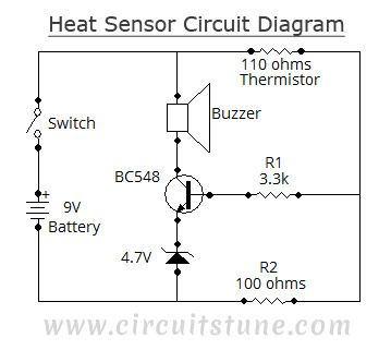
Heat Sensor Circuit Diagram
This simple heat sensor circuit could senses heat from various electronics device like computer, amplifier etc. and generate warning alarm. It could senses heat from environment also, but here I mention “electronics device” because it is being using mostly in electronic device to protect them from overheat.
Circuit diagram of heat sensor:
 |
| Fig-1: Schematic Circuit Diagram Of Heat/Temperature Sensor |
Thermistor, 110 Ohms:
 |
| Fig-2: 110 Ohms Thermistor |
As it is a heat sensor circuit, here a thermistor is used as a heat sensor. It is a thermal measurement device and has a variety of usages including temperature sensor/ heat sensor. The thermistor used in this circuit is a NTC (Negative Temperature Coefficient) type thermistor. When temperature increases, its resistance goes decrease. Therefore, NTC thermistor’s resistances are inverse of temperature.
Circuit Description:
You have seen, in this simple circuit diagram of heat sensor, a few number of components is used including a BC548 transistor, a 110 ohms thermistor etc.- BC548: BC548 is a TO-92 type NPN transistor, as its alternative you can use 2N2222, BC238, BC548, BC168, BC183 etc. they all have almost same characteristic.
- 110 Ohms Thermistor: A 110 Ohms thermistor is used to detecting heat. I have told already about it.
- Buzzer: A buzzer is used with +9V and collector of transistor. When the temperature/ heat exceeds a certain level then it make an alarm.
- 4.7V Zener diode: It is used to limit the emitter current of BC548.
- 9V Battery: A 9V battery is used as a single power source.
- R1, R2: A 3.3K 1/4w resistor is used as R1 and 100 ohms 1/4w as R2.
- Switch: Here in this circuit the switch used is a simple SPST switch. You can either use the switch or not, choice is yours. It is not mandatory.
Tuesday, October 8, 2013
AF Amplifier With Digital Volume Control Based On TDA8551
The Philips Semiconductors TDA8551 is a small audio amplifier with an integrated volume control. When operated from +5 V, it delivers a nominal output power of more than one watt into 8 ohms. It can also be used over a supply voltage range of +2.7 to +5.5 V, with correspondingly reduced output power. The output volume can be adjusted from –60 dB to +20 dB in 64 steps, using a set of up and down push-buttons. The shared UP/DOWN input for the up and down switches has three states. If it is ‘floating’, which means that both of the switches are open, the volume remains unchanged. A pulse to earth decreases the volume by 1.25 dB, while a positive pulse increases the volume by 1.25 dB.
 When the power is switched on, the internal counter takes on the –20 dB setting. An additional input (MODE) allows the amplifier to be switched from the operating state to the mute or standby state. If this input is held at the earth level, the amplifier is operational. If +5 V is applied to this pin, the TDA8551 enters the Standby mode, in which the current consumption drops from the typical operational level of 6mA to less than 10µA. Finally, the MODE input can be used as a mute input by applying a voltage of 1 t0 3.6 V to this input. This voltage can be provided by a connection to the SCR pin, which lies at half of the operating voltage and to which a filter capacitor is connected.
 The loudspeaker is connected in a floating configuration between the two outputs of the bridge amplifier in the TDA8551. This provides the desired output power level, in spite of the low supply voltage. For headphone applications, which do not need as much output power, you can connect the headphone between earth and one of the outputs, via an electrolytic coupling capacitor. You can make a stereo headphone amplifier in this way, using two TDS8551 ICs. The TDA8551 is housed in a DIP8 package. The SMD version is the TDA8551T, in an SO8 package.
More...
 When the power is switched on, the internal counter takes on the –20 dB setting. An additional input (MODE) allows the amplifier to be switched from the operating state to the mute or standby state. If this input is held at the earth level, the amplifier is operational. If +5 V is applied to this pin, the TDA8551 enters the Standby mode, in which the current consumption drops from the typical operational level of 6mA to less than 10µA. Finally, the MODE input can be used as a mute input by applying a voltage of 1 t0 3.6 V to this input. This voltage can be provided by a connection to the SCR pin, which lies at half of the operating voltage and to which a filter capacitor is connected.
 The loudspeaker is connected in a floating configuration between the two outputs of the bridge amplifier in the TDA8551. This provides the desired output power level, in spite of the low supply voltage. For headphone applications, which do not need as much output power, you can connect the headphone between earth and one of the outputs, via an electrolytic coupling capacitor. You can make a stereo headphone amplifier in this way, using two TDS8551 ICs. The TDA8551 is housed in a DIP8 package. The SMD version is the TDA8551T, in an SO8 package.
Sunday, October 6, 2013
UPS For Cordless Telephones
Cordless telephones are very popular nowadays. But they have a major drawback, i.e. they cannot be operated during power failure. Therefore usually another ordinary telephone is connected in parallel to the cordless telephone. This results in lack of secrecy. UPS is a permanent solution to this problem. Since the UPS is meant only for the cordless telephone, its output power is limited to around 1.5W. This is sufficient to operate most cordless telephones. as these employ only small capacity adapters (usually 9V/12V, 500mA), to enable the operation of the circuit and to charge the battery present in the handset. The UPS presently designed is of online type. Here the inverter is ‘on’ throughout, irrespective of the presence of the AC mains.
When the AC mains is present, the same is converted into DC and fed to the inverter. A part of the mains rectified output is used to charge the battery. When the mains power fails, the DC supply to the inverter is from the battery and from this is obtained AC at the inverter output. This is shown in fig.1. The circuit wired around IC CD4047 is an astable multivibrator operating at a frequency of 50 Hz. The Q and Q outputs of this multivibrator directly drive power MOSFETS IRF540. The configuration used is push-pull type. The inverter output is filtered and the spikes are reduced using MOV (metal oxide varistor). The inverter transformer used is an ordinary 9V-0-9V, 1.5A mains transformer readily available in the market.
 Two LEDS (D6 and D7) indicate the presence of mains/battery. The mains supply (when present) is stepped down, rectified and filtered using diodes D1 through D4 and capacitor C1. A part of this supply is also used to charge the battery. In place of a single 12V, 4Ah battery, one may use two 6V, 4Ah batteries (SUNCA or any other suitable brand). The circuit can be easily assembled on a general-purpose PCB and placed inside a metal box. The two transformers may be mounted on the chassis of the box. Also, the two batteries can be mounted in the box using supporting clamps. The front and back panel designs are shown in the Fig. 3. The same circuit can deliver up to 100W, provided the inverter transformer and charging transformer are replaced with higher current rating transformers, so that the system can be used for some other applications as well.
More...
When the AC mains is present, the same is converted into DC and fed to the inverter. A part of the mains rectified output is used to charge the battery. When the mains power fails, the DC supply to the inverter is from the battery and from this is obtained AC at the inverter output. This is shown in fig.1. The circuit wired around IC CD4047 is an astable multivibrator operating at a frequency of 50 Hz. The Q and Q outputs of this multivibrator directly drive power MOSFETS IRF540. The configuration used is push-pull type. The inverter output is filtered and the spikes are reduced using MOV (metal oxide varistor). The inverter transformer used is an ordinary 9V-0-9V, 1.5A mains transformer readily available in the market.
 Two LEDS (D6 and D7) indicate the presence of mains/battery. The mains supply (when present) is stepped down, rectified and filtered using diodes D1 through D4 and capacitor C1. A part of this supply is also used to charge the battery. In place of a single 12V, 4Ah battery, one may use two 6V, 4Ah batteries (SUNCA or any other suitable brand). The circuit can be easily assembled on a general-purpose PCB and placed inside a metal box. The two transformers may be mounted on the chassis of the box. Also, the two batteries can be mounted in the box using supporting clamps. The front and back panel designs are shown in the Fig. 3. The same circuit can deliver up to 100W, provided the inverter transformer and charging transformer are replaced with higher current rating transformers, so that the system can be used for some other applications as well.
Friday, October 4, 2013
SEMICONDUCTOR FMS6363 LOW COST VIDEO FILTER ELECTRONIC DIAGRAM

SEMICONDUCTOR FMS6363 LOW COST VIDEO FILTER ELECTRONIC DIAGRAM
The FMS6363 Low Cost Video Filter (LCVF) provides 6dB gain from input to output. In addition, the input will be slightly offset to optimize the output driver performance. The FMS6363 provides an internal diode clamp to support AC-coupled input signals. If the input signal does not go below ground, the input clamp will not operate. This allows DAC outputs to directly drive the FMS6363 without and AC coupling capacitor (usually 220 ?F). The offset is held to the minimum required value to decrease the standing DC current into the load.
Wednesday, October 2, 2013
12 24 48 V D C Tester
The present tester is intended primarily for testing the 24 V electrical circuits found on most pleasure craft. However, if the resistors are given different values, the circuit may, of course, be used for other voltage ranges. For 12 V, the value of the resistors should be 1.2 k?, and for 48 V, 4.7 k?. The tester should be connected to the +ve and –ve voltage rails with test clips or crocodile clips, whereupon the test probe is placed on the point to be tested. When the potential at the point is positive, the red LED lights; if it is negative, the green one does. If the supply is not connected to earth, the tester may be used as ground-leak tester. In this situation, one of the LEDs lights when the test probe touches a point at earth potential and there is a leakage.

More...

Monday, September 30, 2013
12V Glow Plug Converter
Most small internal-combustion engines commonly used in the model-building world use glow plugs for starting. Unfortunately, glow plugs have an operating voltage of 1.5 V, while fuel pumps, starter motors, chargers and the like generally run on 12 V. This means that a separate battery is always needed to power the glow plug. The standard solution is to use an additional 2-V lead storage battery, with a power diode in series to reduce the voltage by approximately 0.5 V. However, this has the annoying consequence that more than 30 percent of the energy is dissipated in the diode. Naturally, this is far from being efficient. The converter presented here allows glow plugs to be powered from the 12-V storage battery that is usually used for fuelling, charging, starting and so on.
 A car battery can also be used as a power source. Furthermore, this circuit is considerably more efficient than the approach of using a 2-V battery with a series power diode. The heart of the DC/DC converter is IC1, a MAX 1627. The converter works according to the well-known step-down principle, using a coil and an electrolytic capacitor. Here the switching stage is not integrated into the IC, so we are free to select a FET according to the desired current level. In this case, we have selected a 2SJ349 (T1), but any other type of logic-level FET with a low value of RDSon would also be satisfactory. Of course, the FET must be able to handle the required high currents. Diode D1 is a fast Schottky diode, which must be rated to handle the charging currents for C2 and C3. This diode must also be a fairly hefty type. The internal resistances of coil L1 and capacitors C2 and C3 must be as low as possible. This ensures efficient conversion and prevents the components from becoming too warm. The resistor network R2/R3 causes 87 percent of the output voltage to be applied to the FB pin of IC1.
This means that an output voltage of 1.5 V will cause a voltage of approximately 1.3 V to be present at the FB pin. The IC always tries to drive the switching stage such that it ‘sees’ a voltage of 1.3 V on the FB input. If desired, a different output voltage can be provided by modifying the values of R2 and R3. When assembling the circuit, ensure that C5 and C1 are placed as close as possible to IC1, and use sufficiently heavy wiring between the 12-V input and the 1-5-V output, since large currents flow in this part of the circuit. A glow plug can easily draw around 5 A, and the charging current flowing through the coil and into C2 and C3 is a lot higher than this!
More...
 A car battery can also be used as a power source. Furthermore, this circuit is considerably more efficient than the approach of using a 2-V battery with a series power diode. The heart of the DC/DC converter is IC1, a MAX 1627. The converter works according to the well-known step-down principle, using a coil and an electrolytic capacitor. Here the switching stage is not integrated into the IC, so we are free to select a FET according to the desired current level. In this case, we have selected a 2SJ349 (T1), but any other type of logic-level FET with a low value of RDSon would also be satisfactory. Of course, the FET must be able to handle the required high currents. Diode D1 is a fast Schottky diode, which must be rated to handle the charging currents for C2 and C3. This diode must also be a fairly hefty type. The internal resistances of coil L1 and capacitors C2 and C3 must be as low as possible. This ensures efficient conversion and prevents the components from becoming too warm. The resistor network R2/R3 causes 87 percent of the output voltage to be applied to the FB pin of IC1.
This means that an output voltage of 1.5 V will cause a voltage of approximately 1.3 V to be present at the FB pin. The IC always tries to drive the switching stage such that it ‘sees’ a voltage of 1.3 V on the FB input. If desired, a different output voltage can be provided by modifying the values of R2 and R3. When assembling the circuit, ensure that C5 and C1 are placed as close as possible to IC1, and use sufficiently heavy wiring between the 12-V input and the 1-5-V output, since large currents flow in this part of the circuit. A glow plug can easily draw around 5 A, and the charging current flowing through the coil and into C2 and C3 is a lot higher than this!
Saturday, September 28, 2013
BURGLAR ALARM USING IC TIMER 555 556 ELECTRONIC DIAGRAM

BURGLAR ALARM USING IC TIMER 555/556 ELECTRONIC DIAGRAM
circuit diagram of burglar alarm using IC timer 555/556 is functioned as an alarm to prevent thief entering your house. The alarm would produce loud sound when a thin wire connecting resistor R1 with IC pin no 4 is broken. Thin fiber is used as the wire. The thinner the wire, the more responsive the alarm. This circuit needs 5-15V power supply, buzzer is used as a speaker. Here is the circuit schematic :
Parts list :
- Resistor R1 : 10k
- Resistor R2 : 68k
- Resistor R3 : 1k
- Polar capacitor C1 : 1uF/15 B
- Capacitor C2-C3 : 0.01uF
- IC Timer : NE555
Thursday, September 26, 2013
USB Powered PIC Programmer
This simple circuit can be used to program the PIC16F84 and similar "flash memory" type parts. It uses a cheap 555 timer IC to generate the programming voltage from a +5V rail, allowing the circuit to be powered from a computer’s USB port. The 555 timer (IC1) is configured as a free-running oscillator, with a frequency of about 6.5kHz. The output of the timer drives four 100nF capacitors and 1N4148 diodes wir-ed in a Cockroft-Walton voltage multiplier configuration.
Circuit diagram:

The output of the multiplier is switched through to the MCLR/Vpp pin of the PIC during programming via a 4N28 optocoupler. Diodes ZD1 and D5 between the MCLR/Vpp pin and ground clamp the output of the multiplier to about 13.6V, ensuring that the maximum input voltage (Vihh) of the PIC is not exceeded. A 100kΩ resistor pulls the pin down to a valid logic low level (Vil) when the optocoupler is not conducting. The circuit is compatible with the popular "JDM" programmer, so can be used with supporting software such as "ICProg" (see http://www.ic-prog.com).
Author: Luke Weston - Copyright: Silicon Chip Electronics
Tuesday, September 24, 2013
Car Bulb Power Flasher
Derived from the Two-wire Lamp Flasher design, hosted on RED Free Circuit Designs since 1999, this astonishingly simple circuit allows one or two powerful 12V 21W car bulbs to be driven in flashing mode by means of a power MosFet.
Devices of this kind are particularly suited for road, traffic and yard alerts and in all cases where mains supply is not available but a powerful flashing light is yet necessary.
Circuit Diagram:
 Car Bulb Power Flasher Circuit Diagram
| Parts | Description |
| R1 | 6.8K |
| R2 | 220K |
| R3 | 22K |
| C1 | 100uF-25V |
| C2 | 10u-25V |
| D1 | 1N4002 |
| Q1 | BC557 |
| Q2 | IRF530 |
| LP1 | 12V-21W Car Filament Bulb (See Notes) |
| SW1 | SPST Switch (3 Amp minimum) |
Notes:
- Flashing frequency can be varied within a limited range by changing C1 value.
- As high dc currents are involved, please use suitably sized cables for battery and bulb(s) connections.
Source : www.redcircuits.com
Sunday, September 22, 2013
Accurate Bass Tone Control
A difficult problem in the design of conventional stereo tone controls is obtaining synchronous travel of the potentiometers. Even a slight error in synchrony can cause phase and amplitude differences between the two channels. Moreover, linear potentiometers are often used in such controls, and these give rise to unequal performance by human hearing. Special potentiometers that counter these difficulties are normally hard to obtain in retail shops. A good alternative is a control based on a rotary switch and a discrete potential divider. The problem with this that for good tone control more than six steps are needed, and switches for this are also not readily available. Fortunately, electronic circuits can remove these difficulties.
 The analogue selectors used may be driven by mechanical switches, standard logic circuit or a microcontroller. The selectors used in the present circuit are Type SSM2404 versions from Analogue Devices, which switch noiselessly. Each IC contains four selectors, so that a total of eight are used. The step size is 1.25 dB at 20 Hz with a maximum of 10dB . The circuit can be mirrored with S1, which means that a selection may be made of amplification or attenuation of bass frequencies. The user can choose between attenuation only and extending the range by dividing R9. The control can be bridged by switch S2.
To prevent the output impedance of the circuit having too much effect on the operation of the circuit, the output impedance must be ≤ 10 Ω. Resistor R1 2 protects the circuit against too small a load. At maximum bass amplification at Ui n = 1 V r.m.s., the THD+N <0.001% for a frequency range of 20 Hz to 20kHz and and a bandwidth of 80kHz. The circuit draws a current of about 10 mA.
More...
 The analogue selectors used may be driven by mechanical switches, standard logic circuit or a microcontroller. The selectors used in the present circuit are Type SSM2404 versions from Analogue Devices, which switch noiselessly. Each IC contains four selectors, so that a total of eight are used. The step size is 1.25 dB at 20 Hz with a maximum of 10dB . The circuit can be mirrored with S1, which means that a selection may be made of amplification or attenuation of bass frequencies. The user can choose between attenuation only and extending the range by dividing R9. The control can be bridged by switch S2.
To prevent the output impedance of the circuit having too much effect on the operation of the circuit, the output impedance must be ≤ 10 Ω. Resistor R1 2 protects the circuit against too small a load. At maximum bass amplification at Ui n = 1 V r.m.s., the THD+N <0.001% for a frequency range of 20 Hz to 20kHz and and a bandwidth of 80kHz. The circuit draws a current of about 10 mA.
Friday, September 20, 2013

Thursday, September 12, 2013

 Dual Fuel Control Assembly
 Tuesday, September 10, 2013
The Smallest Arduino Clone Possible
Everybody are making Arduino clones. So I thought I should make THE smallest. I took smallest package atmega88 – 28qfn (5mm x 5mm). Routed smallest possible resonator and as much pads as i could fit on in. The result – Smallest Arduino clone ever! Size is only 7.4mm x 7.4mm! Features include:

- Auto reset
- UART
- SPI
- 4 analog channels
- 1 digital i/o
- one LED
- funny readme with BOM
Wednesday, September 4, 2013
LMD18200 Motor Controller Schematic
Using the LMD18200 3A H-Bridge designed by National Semiconductors for motion control applications can be designed a very simple motor controller electronic project . Ideal for driving DC and stepper motors; the LMD18200 accommodates peak output currents up to 6A. An innovative circuit which facilitates low-loss sensing of the output current has been implemented.
LMD18200 Motor Controller Schematic

This circuit controls the current through the motor by applying an average voltage equal to zero to the motor terminals for a fixed period of time, whenever the current through the motor exceeds the commanded current. This action causes the motor current to vary slightly about an externally controlled average level. The duration of the Off-period is adjusted by the resistor and capacitor combination of the LM555.
Using this motor driver circuit you can design a 24 DC motor that require a maximum current consumption of 3 amperes .
LMD18200 Motor Controller Schematic

Using this motor driver circuit you can design a 24 DC motor that require a maximum current consumption of 3 amperes .
Monday, September 2, 2013
2x6W Stereo Audio Amplifier based LA4440 Power IC
This is the diagram of 2x6W stereo audio amplifier based LA4440 power IC. Actually, the LA4440 can be used in both stereo mode and mono (bridge) mode, but the circuit presented in this post is LA4440 in stereo mode. The recommended power supply is 13.2V, while the maximum voltage rated at 18V.

LA4440 Features:

- Built-in 2 channels (dual) enabling use in stereo and bridge amplifier applications.
- Dual : 6W´2 (typ.)
- Bridge : 19W (typ.)
- Minimum number of external parts required.
- Small pop noise at the time of power supply ON/OFF and good starting balance.
- Good channel separation.
- Good ripple rejection : 46dB (typ.)
- Low distortion over a wide range from low frequencies to high frequencies.
- Small residual noise (Rg=0).
- Easy to design radiator fin.
- Built-in protectors.
- Built-in audio muting function.
- Thermal protector
- Overvoltage, surge voltage protector
- Pin-to-pin short protector
Saturday, August 31, 2013
Pulse Width Modulation DC Motor Control Circuit
Description
 Parts
Parts
Notes
Often, people attempt to control DC motors with a variable resistor or variable resistor connected to a transistor. While the latter approach works well, it generates heat and hence wastes power. This simple pulse width modulation DC motor control eliminates these problems. It controls the motor speed by driving the motor with short pulses. These pulses vary in duration to change the speed of the motor. The longer the pulses, the faster the motor turns, and vice versa.
Circuit Diagram
- R1 1 Meg 1/4W Resistor
- R2 100K Pot
- C1 0.1uF 25V Ceramic Disc Capacitor
- C2 0.01uF 25V Ceramic Disc Capacitor
- Q1 IRF511 MOSFET or IRF620
- U1 4011 CMOS NAND Gate
- S1 DPDT Switch
- M1 Motor (See Notes)
- MISC Case, Board, Heatsink, Knob For R2, Socket For U1
- R2 adjusts the speed of the oscillator and therefore the speed of M1.
- M1 can be any DC motor that operates from 6V and does not draw more than the maximum current of Q1. The voltage can be increased by connecting the higher voltage to the switch instead of the 6V that powers the oscillator. Be sure not to exceed the power rating of Q1 if you do this.
- Q1 will need a heatsink.
- Q1 in the parts list can handle a maximum of 5A. Use the IRF620 for 6A, if you need any higher.
Thursday, August 15, 2013
Simple Cold Cathode Fluorescent Lamp Supply Circuit Diagram
Simple Cold-Cathode Fluorescent-Lamp Supply Circuit Diagram. For back-lit LCD displays, this supply will drive a lamp. LT1072 drives Ql and Q2, and a sine wave appears across CI. LI is a transformer that steps up this voltage to about 1400 V. Dl and D2 detect lamp current and form a feedback loop to the LT1072 to control lamp brightness. C1 = MUST BE A LOW LOSS CAPACITOR. METALIZED POLYCARB WIMA FPK 2 (GERMAN) RECOMMENDED. L1 = SUMIDA 6345-020 OR COILTRONIX CTX110092-1. PIN NUMBERS SHOWN FOR COILTRONIX UNIT. L2 = COILTRONIX CTX300-4 * = 1 % FILM RESISTOR.
Cold-Cathode Fluorescent-Lamp Supply Circuit Diagram

Tuesday, August 13, 2013
1992 BMW 325i Convertible Electrical Troubleshooting Manual Electrical Troubleshooting Wiring Diagram Cable Harness Routing and Electrical Schematics
This electrical troubleshooting manual is divided into following sections: Index, How to Use the Wiring Diagram, Wire Size and Conversion Chart, Symbols, Systematic Troubleshooting, Connectors Views, Power Distribution Box, Fuse Data, Component Location Chart and Views, and Splice Location Views. Further breakdown, this manual covers topics on operation description and systematic troubleshooting for power distribution system, charge and starting system, ABS, Brake Warning System, Power Mirrors, Central Locking, Power Windows, electronics fuel injection system, SRS, Seats, Electro-Mechanical Convertible Top, Body Electrical System, Wiper and Washer, Instrument Cluster, etc.

All wirings and the wiring between components are shown exactly as it exists in the vehicle; but, the wiring is not drawn to scale. Wiring inside complicated components has been simplified to solid state label designates electronic components to help you in understanding the electrical operation,
A complete troubleshooting manual for the 1992 BMW 325i Convertible Electrical Troubleshooting Manual is here – 142 pages of PDF file.
Sunday, August 11, 2013
Fuse Box BMW Z3 Plug in 1996 Diagram
Fuse Box BMW Z3 Plug in 1996 Diagram - Here are new post for Fuse Box BMW Z3 Plug in 1996 Diagram.


Fuse Panel Layout Diagram Parts: high beam light relay, fuel pump relay, crash control module, auxiliary fuse box.
More...
Fuse Box BMW Z3 Plug in 1996 Diagram


Fuse Panel Layout Diagram Parts: high beam light relay, fuel pump relay, crash control module, auxiliary fuse box.
Friday, August 9, 2013
Wiring Diagram

Rj45 Wiring Diagram T568a.

Rj45 Socket Wiring Reviews And Photos.

Welcome To Tutor Piggy Blogspot Com Rj45 Wiring Diagram.

Rj45 Cat 5 Wiring Diagram For Straight Through Cable.

Wiring Diagram.
Order Of The Bath Churchtech.
Wiring Diagram.

How Hard Is It To Make Your Own Cat 6 Cables Iphone And Ipad Forums.

How To Make Your Own Network Cables Twisted Pair Network Cables.

Rj45 Cat6 Wiring Diagram Submited Images Pic 2 Fly.
Wednesday, August 7, 2013
Invisible Broken Wire Detector
Portable loads such as video cameras, halogen flood lights, electrical irons, hand drillers, grinders, and cutters are powered by connecting long 2- or 3-core cables to the mains plug. Due to prolonged usage, the power cord wires are subjected to mechanical strain and stress, which can lead to internal snapping of wires at any point. In such a case most people go for replacing the core/cable, as finding the exact location of a broken wire is difficult.
In 3-core cables, it appears almost impossible to detect a broken wire and the point of break without physically disturbing all the three wires that are concealed in a PVC jacket. The circuit presented here can easily and quickly detect a broken/faulty wire and its breakage point in 1-core, 2-core, and 3-core cables without physically disturbing wires. It is built using hex inverter CMOS CD4069.
Gates N3 and N4 are used as a pulse generator that oscillates at around 1000 Hz in audio range. The frequency is determined by timing components comprising resistors R3 and R4, and capacitor C1. Gates N1 and N2 are used to sense the presence of 230V AC field around the live wire and buffer weak AC voltage picked from the test probe. The voltage at output pin 10 of gate N2 can enable or inhibit the oscillator circuit.
When the test probe is away from any high-voltage AC field, output pin 10 of gate N2 remains low. As a result, diode D3 conducts and inhibits the oscillator circuit from oscillating. Simultaneously, the output of gate N3 at pin 6 goes ‘low’ to cut off transistor T1. As a result, LED1 goes off. When the test probe is moved closer to 230V AC, 50Hz mains live wire, during every positive half-cycle, output pin 10 of gate N2 goes high.
Thus during every positive half-cycle of the mains frequency, the oscillator circuit is allowed to oscillate at around 1 kHz, making red LED (LED1) to blink. (Due to the persistence of vision, the LED appears to be glowing continuously.) This type of blinking reduces consumption of the current from button cells used for power supply. A 3V DC supply is sufficient for powering the whole circuit.
Circuit diagram:

Invisible Broken Wire Detector Circuit Diagram
AG13 or LR44 type button cells, which are also used inside laser pointers or in LED-based continuity testers, can be used for the circuit. The circuit consumes 3 mA during the sensing of AC mains voltage. For audio-visual indication, one may use a small buzzer (usually built inside quartz alarm time pieces) in parallel with one small (3mm) LCD in place of LED1 and resistor R5. In such a case, the current consumption of the circuit will be around 7 mA.
Alternatively, one may use two 1.5V R6- or AA-type batteries. Using this gadget, one can also quickly detect fused small filament bulbs in serial loops powered by 230V AC mains.
The whole circuit can be accommodated in a small PVC pipe and used as a handy broken-wire detector. Before detecting broken faulty wires, take out any connected load and find out the faulty wire first by continuity method using any multimeter or continuity tester.
Then connect 230V AC mains live wire at one end of the faulty wire, leaving the other end free. Connect neutral terminal of the mains AC to the remaining wires at one end. However, if any of the remaining wires is also found to be faulty, then both ends of these wires are connected to neutral. For single-wire testing, connecting neutral only to the live wire at one end is sufficient to detect the breakage point.
In this circuit, a 5cm (2-inch) long, thick, single-strand wire is used as the test probe. To detect the breakage point, turn on switch S1 and slowly move the test probe closer to the faulty wire, beginning with the input point of the live wire and proceeding towards its other end. LED1 starts glowing during the presence of AC voltage in faulty wire. When the breakage point is reached, LED1 immediately extinguishes due to the non-availability of mains AC voltage.
The point where LED1 is turned off is the exact broken-wire point. While testing a broken 3-core rounded cable wire, bend the probe’s edge in the form of ‘J’ to increase its sensitivity and move the bent edge of the test probe closer over the cable. During testing avoid any strong electric field close to the circuit to avoid false detection.
Author: K. Udhaya Kumaran
Monday, August 5, 2013
Simple Solar LED Lantern
This solar LED lantern can be used as an emergency light. Its 6V battery can be charged either from 230V, 50Hz AC mains or a 12V, 10W solar panel. Two LED indicators have been provided—red LED (LED1) indicates battery charging and green LED (LED2) indicates fully-charged battery.
You can choose to charge the battery either from the mains power or the solar panel by using the single-pole, double-throw (SPDT) switch. Capacitor C1 (1000µF, 35V) removes ripples from the power supply and regulator IC LM7809 (IC1) provides regulated 9V DC to the emitter of pnp transistor T1 (TIP127/BD140) and pin 7 of op-amp IC CA3140 (IC2), which is configured in comparator mode.
The reference voltage of 6.3V at pin 2 of IC2 is obtained through the combination of resistor R7 (1-kilo-ohm) and zener diode ZD1 (6.3V). The comparator controls charging of the battery. Pin 3 of IC2 is connected to the positive terminal of the battery to be charged through resistor R5. When the battery is fully charged, it stops charging and the green LED (LED2) glows to indicate the full-charge status.
When the battery voltage is low, diode D1 (1N4007) forward-biases and the battery connects (through resistor R3) to the collector of T1 for charging (indicated by the glowing of red LED1). Three high-wattage white LEDs (LED3 through LED5), such as KLHP3433 from Kwality Photonics, are used for lighting. These are switched on using switch S3.
You can choose to charge the battery either from the mains power or the solar panel by using the single-pole, double-throw (SPDT) switch. Capacitor C1 (1000µF, 35V) removes ripples from the power supply and regulator IC LM7809 (IC1) provides regulated 9V DC to the emitter of pnp transistor T1 (TIP127/BD140) and pin 7 of op-amp IC CA3140 (IC2), which is configured in comparator mode.
 |
When the battery voltage is low, diode D1 (1N4007) forward-biases and the battery connects (through resistor R3) to the collector of T1 for charging (indicated by the glowing of red LED1). Three high-wattage white LEDs (LED3 through LED5), such as KLHP3433 from Kwality Photonics, are used for lighting. These are switched on using switch S3.
Saturday, August 3, 2013
Simple Cell Phone Jammer Circuit Diagram 2
A beautiful diy gsm jammer or mobile cell phone jammer schematic diagram for use only in GSM1900 with frequency from 1930 MHz to 1990 MHz. The GSM1900 mobile phone network is used by USA, Canada and most of the countries in South America.
This cell phone jammier is not applicable for use in Europe, Middle East, nor Asia. The GSM jammier circuit could block mobile phone signals which works on GSM1900 band, also called DCS. For more cell phone jammers check the related posts.
Mobile cellphone jammer circuit diagram

Thursday, August 1, 2013
1 W Home Stereo Amplifier Rise
This is a one watt home stereo amplifier module project using the KA2209 IC from Samsung, which is equivalent to the TDA2822. It operates from 3-12V DC & will work from a battery since the dormant current drain is low. It requires no heat sink for normal use. The input & output are both ground referenced. Maximum output will be obtained with a 12V power supply & 8 ohm speaker, however it is suitable for driving headphones from a supply as low as 3V.
The Specifications of the home stereo amplifier :
The Specifications of the home stereo amplifier :
D.C. input : 3 – 12 V at 200 – 500 mA max
Idle current : approx. 10 mA
Power output : > 1 Watt max. 4-8 ohms, 12V DC
Freq. Resp. : approx. 40 Hz to 200 kHz, 8 ohm, G=10
THD : < 1 % @ 750 mW, 4-8 ohm, 12V
Gain : approx. x10 (20 dB) OR x100 (40dB)
S/N ratio : > 80 dB, G = 20 dB
Sensitivity : < 300 mV, G = 20 dB
Input Impedance : approx. 10 k ohm
Description
The gain is adjustable from ten to 100, i.e. twenty to 40 dB. Start with feedback resistors R1 and R3 of 1k ohm, this will give a gain of ten which ought to be adequate for most applications. In case you need more gain, you can remove resistors R1 and R3.This will give a gain of about 100, or 40 dB.The input attenuation can be adjusted by the potentiometer which can be used as a volume control. The IC gain ought to be kept as low as necessary to accomplish full output, with the in put potentiometer and your signal source at maximum.

Voltage Gain = 1+ R1/R2 = 1+R3/R4, however the maximum gain with no outside feedback is about 100, or 40dB. (GdB = 20log Gv)
This will keep the signal to noise ratio as high as feasible. Additional gain provided by the amplifier will reduce the S/N ratio by a similar amount, since the input noise figure is constant. Other values for R1 and R3 of between 1k and 10k ohm can be used if an intermediate gain level is necessary.
This will keep the signal to noise ratio as high as feasible. Additional gain provided by the amplifier will reduce the S/N ratio by a similar amount, since the input noise figure is constant. Other values for R1 and R3 of between 1k and 10k ohm can be used if an intermediate gain level is necessary.
If driving a pair of headphones, you may also need a 100 ohm resistor in series with each output to reduce the output level, depending on headphone impedance & sensitivity. Make positive you start with the volume right down to check. Numerous headphones may be driven from the amplifier in the event you wish, since most headphones have at least 16 ohm impedance, or more often 32 ohm.
There are only a few outside parts, the IC contains most of the necessary circuitry. R1,R2 and R3,R4 are the feedback resistors. C1 provides power supply decoupling. C2 and C3 are the input coupling capacitors, which block any DC that might-be present on the inputs. C4,C5 block DC in the feed back circuit from the inverting inputs, and C6,C7 are the output coupling capacitors. C8, R5 and C9,R6 act as Nobel networks providing a high frequency load to maintain stability at frequencies where loud speaker inductive reactant may become excessive. The pot provides adjustable input level attenuation.

Tuesday, July 30, 2013
Mini Alarm
This circuit, enclosed in a small plastic box, can be placed into a bag or handbag. A small magnet is placed close to the reed switch and connected to the hand or the clothes of the person carrying the bag by means of a tiny cord. If the bag is snatched abruptly, the magnet looses its contact with the reed switch, SW1 opens, the circuit starts oscillating and the loudspeaker emits a loud alarm sound. A complementary transistor-pair is wired as a high efficiency oscillator, directly driving a small loudspeaker. Low part-count and 3V battery supply allow a very compact construction.

Parts:
R1 = 330K
R2 = 100R
C1 = 10nF-63V
C2 = 100uF-25V
Q1 = BC547
Q2 = BC327
B1 = 3V Battery or Two AA Cells in Series
SW1 = Read Switch & Small Magnet
SPKR = 8R Loudspeaker (See Notes)
Notes:
* The loudspeaker can be any type; its dimensions are limited only by the box that will enclose it.
* An on-off switch is unnecessary because the stand-by current drawing is less than 20µA.
* Current consumption when the alarm is sounding is about 100mA.
* If the circuit is used as anti-bag-snatching, SW1 can be replaced by a 3.5mm mono Jack socket and the magnet by a 3.5mm. Mono Jack plugs having its internal leads shorted. The Jack plug will be connected to the tiny cord etc.
* Do not supply this circuit at voltages exceeding 4.5V: it will not work and Q2 could be damaged. In any case a 3V supply is the best compromise.
More...
Parts:
R1 = 330K
R2 = 100R
C1 = 10nF-63V
C2 = 100uF-25V
Q1 = BC547
Q2 = BC327
B1 = 3V Battery or Two AA Cells in Series
SW1 = Read Switch & Small Magnet
SPKR = 8R Loudspeaker (See Notes)
Notes:
* The loudspeaker can be any type; its dimensions are limited only by the box that will enclose it.
* An on-off switch is unnecessary because the stand-by current drawing is less than 20µA.
* Current consumption when the alarm is sounding is about 100mA.
* If the circuit is used as anti-bag-snatching, SW1 can be replaced by a 3.5mm mono Jack socket and the magnet by a 3.5mm. Mono Jack plugs having its internal leads shorted. The Jack plug will be connected to the tiny cord etc.
* Do not supply this circuit at voltages exceeding 4.5V: it will not work and Q2 could be damaged. In any case a 3V supply is the best compromise.
Monday, July 29, 2013
Alternator Wiring Questionpage450965

1990 Mercruiser 350 Alternator Wiring Diagram.

Magazin Componente Electronice Cluj Anode Half Reaction.
Alternator Wiring.

68 Charging At 14 8v And Acid Leaking From The Battery Vintage.
Serpentine Alternator Wiring.

Please Note The Fuse Wire Connected To The Starter Solenoid And Not.

Marine Alternator Diagram Mando Alternator Wire Marine Alternator.

Alternator Wiring Question Page 1 450965.
Alternator Regulator Troubleshooting.

Alternator Bracket For The Top Mounting About 15 On Line The Wiring.
Subscribe to:
Posts (Atom)