Tuesday, April 30, 2013

Improvised Fan Grills

Making your own grill for your fans would be a lot easier and cheaper. You could use all materials that can be found in your home.

Hacks and Mods: Improvised Fan Grills

Your main component would be your old fan, removed its metal ring and you can now measure the desired length or size of grid that you will be needed. Cut the grid across so it will be easier to cut, then place it in the tower and use the same screw you removed in the fan.

Hacks and Mods: Improvised Fan Grills

Now you can put the grid holding fan back in its place. Clean up and you can now use your very own fan grills that cost almost nothing but your patience.
More...

Saturday, April 13, 2013

Variable 0 to 300 Volts Regulated Power Supply Circuit Diagram

This power supply can be used to  obtain a regulated power output, variable right from zero to 300 volts maximum. All the devices should be mounted on heatsinks.


You must have come across many power supply circuits which are designed for supplying anywhere between 0 to 25 or at the most 40 volts DC, but the circuit presented here will give you a robust power right from 0 to 300volts continuously variable.

The circuit diagram can be understood with the following points:

As can be seen in the figure, a high voltage transistor BF458 is used as the main load handling device.
Its base bias is controlled by another high voltage transistor BF337 whose emitter is clamped to a stable 24 volts.

An FET is used for selecting the base current of the transistor BF337 via a pot of 1M.

This setting adjusts the base current for the BF337 which in turn restricts the main transistor BF458s voltage and current flow to the output.

The input to the circuit may be derived directly from the mains AC after proper rectification and filtration using a bridge network and a 10u/400V capacitor.

The entire circuit is extremely dangerous to touch, due care should be maintained while making and testing this circuit.


More...

Wireless Baby Monitor

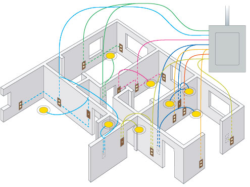
Walkie-talkies (also often referred to as handheld or PMR, Personal Mobile Radio) can be bought at low prices even from department retailers, and they are able to be operated with no licence in many international vicinitys. Considering the low value, such a set can be very appropriate to be used as a wireless baby reveal, with the addition of a few external components. These are linked to the jack sockets for an exterior loudspeaker/microphone and an external PTT (Push-To-Talk) change, which would possibly be incessantly discovered on these tools. 

Project Image :
Wireless Baby Monitor Project Image

The walkie-talkie with the additional digitals and microphone is positioned within the baby’s room. When the PTT switch on the opposite walkie-talkie is actuated for approximately a 2d the ‘baby’ walkie-talkie produces a sequence of tones, which the exterior electronics can observe. This then prompts its own PTT swap for roughly 5 2ds, so it swapes over to transmit. During this time the different instrument can hear what the exterior microphone picks up. 

Circuit Diagram :
Figure 1-Wireless Baby Monitor Circuit Diagram

Figure 1 shows the circuit that the writer designed for this. It has been designed namely for a Tevion three000 PMR bought a while ago with the help of Aldi. This kind of PMR has a combined jack socket that embraces all the required connections. 

The voltage present on the PTT connector is used to generate the provision voltage for the circuit by the use of R3, D1 and C1/C2. When the loud-speaker output presents a sequence of tones (when the PTT change on the opposite walkie-talkie is held down), it lead tos T1 to behavior. This also turns on T2 and T3, so that the external microphone is related to floor. The ensuing present that f lows through the microphone must be sufficient to prompt the PTT circuit within the walkie-talkie, inflicting it to transmit. If the external microphone doesn’t draw sufficient present, a resistor (R8) will have to be linked in parallel. Some experimentation with the worth of this resistor may be required. If you are looking to have to make use of the inner microphone then R8 should get replaced with a wire hyperlink. 

Circuit diagram :
Figure 2-Wireless Baby Monitor Circuit Diagram

When the walkie-talkie changees to transmit the built-in amplifier ceases producing a sign and T1 flips off. However, due to the fact electrolytic capacitor C3 has been charged up in the interim, transistors T2 and T3 will preserve habitsing for a couple of seconds until C3 has been virtually discharged via R4. In the Elektor labs a more practical version with the identical functionality (Figure 2) has been designed for use with a more cost effective PMR set that is additionally received from Conrad Electronics (PMR Pocket Comm Active Pair, order number 930444). These walkie-talkies have separate jack sockets for the LS/Mic and PTT joinions. 

When there is a call a series of tones is produced that is used to activate T1 by means of R3. T1 then prompts the PTT perform and the microphone amplifier is turned on. How-ever, it ’s not just the audio sign that's used, but additionally the DC offset produced when the interior output stage is turned on. Both the interior in addition to external loudspeaker are pushed by means of an output capacitor of a hundred µF. When there's a call it charges up by means of R3 and the base-emitter junction of T1. If the walkie-talkie is known as frequently there could be a risk that the output capacitor would remain charged and the DC offset of the audio signal would now not be sufficient to activate T1. To prevent this, D1 is hooked up in reverse across the base-emitter junction of T1, pro-viding a discharge path for the output capacitor.

To maintain the circuit energetic for a minimum period of time the microphone voltage is used to supply an additional base present. This is finished by means of charging C1 by approach of R1. When the transmitter is fliped off the microphone and R2/ D1 provide a discharge path for the capacitor. C2 make certain thats that the circuit won’t react to spikes resulting from interference. As can also be seen from the 2d circuit diagram, use is manufactured from two joinors, a 2.5 mm jack plug for an exterior headset and a 3.5 mm plug for the PTT perform. These joinors are explicit to the walkie-talkies we used right here. With other types of walkie-talkie you must first take a seem to be at the joinion important points of the connectors sooner than you connect the circuit up. 

When the circuit is used as a child monitor you should test that the microphone you’re the use of can decide up all the sounds. In our case the microphone didn’t seem like very sensitive. The microphone amplifier has almost definitely been designed for a voice that's close to the PMR unit. When used as a child screen the microphone must subsequently be placed as with reference to the infant as that that you can suppose of.


Author : Wolfgang Papke - Ton Giesberts
More...

Luminescent Generator

When spun abruptly between the fingers, a bipolar stepper motor will generate around 10VAC. If this is stepped up with a small 240V to 6-0-6V transformer in reverse (with collection related secondaries), a small bipolar stepper motor is in a position to powering a standard 5cm through 6cm luminescent sheet at full brightness. These are designed to be powered from 20V to 200VAC (typically 115VAC), producing 1.5 candelas of light - that will dimly light the common room, or competently mild a camp desk. They are manufactured through Seikosha (RS Components Cat. 267-8726).

Circuit diagram:
Luminescent Generator Circuit Diagram

The transformer will have to be a small one (around 100mA or so), in any other case effectivity is compromised. The wires of the motors two segments are regularly paired white & yellow and red & blue. Just some of these sections is employed in the circuit. If a small bipolar stepper motor from a discarded three.5-inch disk power is used, the Luminescent Generator is also constructed into an extraordinarily small enclosure. To maintain speedy, easy spinning of the motor, a geared deal with could also be brought.


Author: Thomas Scarborough - Copyright: Silicon Chip
More...

Mains AC Xenon Tube Flasher Circuit

The article discusses a very simple yet amusing mains operated xenon tube flasher circuit using ordinary electronic components.


The circuit was taken from one of the old elektor electronics magazine and it is indeed a very cute little circuit which may be used for creating high intensity lighting effects during festivals, parties and fun gatherings.

The circuit may be understood by referring to the diagram and with the following explanations:

Diodes D1 and D2 along with the capacitors C1 and C2 form a voltage doubler circuit which creates a voltage level twice the value of the input voltage (across C1/C2).

Resistors R4 along with R5 and P1 provides the gate current to the triac so that it can fire for the required actions.

However the triac is unable to fire until the voltage reaches above the diac firing voltage which is around 60 volts (due to D3/D4).

Once this happens the triac triggers, inducing a momentary pulse inside the primary winding of the pulse transformer via C3.

This in turn jumps a high voltage pulse into the secondary of the  transformer which is connected to the trigger wire of the xenon bulb.

The xenon bulb triggers due to the above actions passing the entire voltage across C1/C2 through it.
This generates a blinding arc light inside the tube, producing the required high intensity flash.

However once the tube fires C1/C2 completely discharges making the gate voltage of the triac fall to zero switching OFF the xenon bulb instantly

The whole circuit returns to its original condition until C1/C2 charges up again and repeats the cycle.

Thus the flashing keeps repeating as long as mains power stays connected at the input.


Xenon Tube

As the name suggests, its a tube filled with inert xenon gas. A metal ring is attached toward the anode side of the tube which becomes the gate trigger point of the device. This ring is terminated with a wire so that it can be connected with s pulse source.

When a high voltage is set across the anode/cathode pins of the tube and a pulse applied across the trigger gate wire and cathode, the tube gets charged up and allows the whole voltage across its Anode.cathode to pass through creating an intense arc lighting inside the tube due to the passage of the high speed electrons through the xenon gas.

Any standard xenon tube can be used here, preferably the ones which are used in electronic cameras.

The transformer

The transformer may be built by winding 100 turns of 36 SWG wire over a tiny ferrite core. This becomes the secondary winding (A to B)

And about 10 turns of 22 SWG over the above winding. This becomes the primary winding of the transformer (A to C)
More...

50W Electronic Amplifier Rise

This electronic amplifier project is an IC amplifier module from ST Microelectronics, the TDA7294. It is intended for use as a prime quality audio classification AB amplifier in hi-fi softwares. Its low noise and distortion, broad bandwidth and good output present functionality, enabling it to produce excessive power in to each four ohm and 8 ohm heaps. Its each quick circuit and thermal protection.

With the addition of a handful of sections and the appropriate power provide, this module will deliver over 50W RMS in to four or eight ohms-with < 0.1% Total Harmonic Distortion (THD) and < 0.1% Inter-modulation Distortion (IMD). It can also be appropriate as a replacement power amp stage, or improve for loads of existing amplifiers of between 30W-50W, provided they have got the precise twin provide, & most do.

The Specifications of the digital amplifier project there are:

D.C. Input : 35V
Output energy : > 50W RMS, 4-8 ohm load.
Gain : 24 dB (30dB modification)
Input sensitivity : one.3V for 50W, 8 ohm
Signal-to-Noise ratio : > ninety five dB, (>105 dBA)
Frequency response : approx. 20Hz - 200kHz, �3 dB
Slew charge : > 10V/uS
THD : < 0.01%, 1W-40W, 1kHz
IMD : < zero.01%, 1W

The maximum provide voltage of the IC is +/- 40V. However the most dissipation of the IC can be exceeded even at a lower voltage. Therefore the provide voltage used require now not be over +/- 35V. This may additionally be developed the utilization of a 50V heart tapped-transformer, a diode bridge rated at 5A (min.) & a pair of electrolytic capacitors, as shown under. A lower secondary voltage transformer may even be used however the reduced DC voltage will lead to less energy output in to 8 ohms. You can still receive 50W in to four ohms with best 24V supply rails.

A 36V C.T. transformer offers you approx +/- 25V rails. The-mains transformer used must be feed at a most of 80VA. In the experience you require to run modules in a stereo amplifier you want to use a typical power supply. In this case the transformer ought to be charged at 150VA or higher.


Electronic Amplifier Circuit Diagram Description

Most of the circuitry is contained throughout the IC module. The enter sign is applied to pin three by capacitor C1 & low-pass filter R1/C2. The filter strengthens the coronary heart beat response & lend a hands stop RF indicators. The lower -3dB point is determined-by R2/C1 & R4/C3. This is set 20Hz for the values used. The higher -3dB point is over 200kHz. C7/C8 & C9/C10 provide further power provide filtering or decoupling.


R3/R4 are the feedback resistors. The achieve is 1+R3/R4 which is approx 16 times, or 24dB. In case you wish to elevate the enter sensitivity you can additionally alter the resistors to swimsuit. Changing R3 to 22k would elevate the acquire to 30dB and lower the enter-required for 50W in to eight ohm, to 0.6V, without affecting efficiency so much. In case you scale back the worth of R4 you are going to additionally need to raise C3 to maintain bass response, as this units the comments low frequency roll off.

Pin ten is a mute enter and pin 9 gives a standby mode. Muting ought to always happen earlier than standby mode is chosen. Connecting these pins completely to the provision rail ensures that the amplifier comes on right away on energy up. Any switch-on clicks may be eradicated by means of increasing the time constants of R5/C4 and R6/C5 if necessary.

Make definite that a heavy accountability heat-sink charged as a minimum one.4 stage C/W or higher is used.


More...

Friday, April 12, 2013

Cheapest Ever Motion Sensor

The RS-455-3671 sensor used in the Automatic Rear Bicycle Light challenge printed in  the July/August 2010 model will additionally be replaced by way of a motion sensor that prices nothing instead of a fiver or thereabouts. 

 
The replacement is a do-it-yourself device, constructed from elements simply found within the workshop of any digitals fanatic. Effectively it works as a variable resistor, depending on the acceleration force to which the software is  submitted. A prototype introduced a resistance of 200 kΩ when now not shifting, and a hundred ninety kΩ when shedding about 1 cm.

Constructing is easy. Cut off a bit of about 10 mm of copper tubing. Take a bit of conductive foam, the kind used to supply safety to integrated circuits. Cut a rectangular piece of 10  x 50 mm. Roll up firmly except it may additionally be push-fitted securely into the copper cylinder. Then insert a conductive wire in the direction of the centre of the cylinder, bend it and (optionally) add protective plastic sleeving to each and every side. This is the first contact. Finally, solder a skinny wire to the copper cylinder. This is the second contact. The foam resistance is stress based. 

Consequently, when the tool transfers due to an external power, the inertia of the cylinder lead tos varying pressure within the foam, leading to a small change of resistance between the interior conductor and  the cylinder. Because of that, it’s necessary to verify the cylinder vibration shouldn't be limited in any way through the connecting wire or the PCB. 

The comparator circuit proven right here is able to resolving the resistance change of the proposed foam/wire/copper sensor, permitting it to become mindful of the motion of a automobile for alarm or different functions. 


Author : Antoni Gendrau – Copyright : Elektor
More...

Simple Rain Alarm or Water Detector Circuit with SCR 106CY

Rain detector circuit may also be utilized to the challenge or any other pastime, rnwhich is so easy principles.When it rains plate (sensor) will receive rnrain. And a faithful work has paid to SCR1 and go with the flow preserve watch over Buzzer rnnoise.
Electronic Part List 

R1 1K 1/4 W Resistor
R2 680 Ohm 1/4 W Resistor
D1 1N4001 Silicon Diode
BZ1 12V Buzzer
S1 SPST Switch
SCR1 C106B1 SCR 106CY
SENSOR See

Notes  

Thern sensor is a small piece of PC board etched to the pattern showen in thern schematic. The hints must be very shut to every other, however with the aid of no indicates rntouching. A big spiral pattern would additionally work. 2. Make sure to make use of arn loud buzzer
More...

Extend Timer Range For The 555

Anyone who has designed circuits the utilization of the 555 timer chip will, at some time have wished that it may be programmed for longer timing periods. Timing periods better than a few minutes are difficult to reach as a result of component leakage presents in huge timing capacitors turn into vital. There is alternatively no motive to opt for a only digital answer simply but. The circuit proven here uses a 555 timer in the design but nonetheless succeed ins a timing interval of as a lot as an hour! The trick here is to feed the timing capacitor now not with a relentless voltage however with a pulsed dc voltage. The pulses are derived from the un smoothed low voltage output of the ability provide bridge rectifier.The power supply output is just now not referenced to earth possible and the pulsing full wave rectified sign is fed to the bottom of T1 by way of resistor R1. A 100-Hz sq. wave signal is produced on the collector of T1 as the transistor switches.

The sure 1 of 2 of this waveform charges up the timing capacitor C1 via D2 and P1. Diode D2 forestalls the charge on C1 from discharging thru T1 when the sq. wave signal goes low. Push-button S1 is used to start out the timing length. This methodology of charging uses reasonably low component values for P1 (2.2 MΩ) and C1 (100 to 200 µF) but reachs timing durations of up to an hour which is for much longer than a typical 555 circuit configuration.
More...

10W Stereo Audio Amplifier Using TDA2009A

This is a schematic of a 10W stereo audio amplifier using TDA2009A amplifier IC. TDA2009A is a good IC provides quality sound. It has built in features like output current protection and thermal protection etc. The circuit can be operate between 8 to 24V DC with 1 to 2 amphere.

10W Stereo Audio Amplifier Circuit Diagram :

10w-stereo-amplifier-circuit-diagram

If you want to operate this 10 watt amplifier circuit with watt amplifier circuit with mains supply then use a filtered and stable power supply to reduce mains hum. 10 watt out put power can be obtained by providing 20V 1.5A to the circuit. Use good and thick heatsink with the IC.

Source : http://www.ecircuitslab.com/2012/08/10w-stereo-audio-amplifier-using.html

More...

Wireless On Off Switch

Normally home appliances are controlled by means of switches, sensors, etc. However, physical contact with switches may be dangerous if there is any shorting. The circuit described here requires no physical contact for operating the appliance. You just need to move your hand between the infrared LED (D2) and the phototransistor (Q1). 

Wireless On-Off Switch Circuit diagram :


The infrared rays transmitted by D2 is detected by the phototransistor to activate the hidden lock, flush system, hand dryer or else. This circuit is very stable and sensitive compared to other AC appliance control circuits. It is simple, compact and cheap. Current consumption is low in milliamperes. The circuit is built around an IC CA3140, D2, phototransistor and other discrete components.

Parts:
R1 = 470R
R2 = 100K
R3 = 3.3K
R4 = 10K
D1 = 1N4007
D2 = IR LED
Q1 = L14F1
RL = 5Vdc Relay
IC = CA3140
Q2 = BC548

Circuit Operation:

When regulated 5V is connected to the circuit, D2 emits infrared rays, which are received by phototransistor Q1 if it is properly aligned. The collector of Q1 is connected to non-inverting pin 3 of IC1. Inverting pin 2 of IC1 is connected to voltage-divider preset R4. Using preset R4 you can vary the reference voltage at pin 2, which also affects sensitivity of the phototransistor. Op-amp IC1 amplifies the signal received from the phototransistor. Resistor R3 controls the base current of transistor BC548 (Q2). The high output of IC1 at pin 6 drives transistor Q2 to energies relay RL1 and switch on the appliance, say, hand dryer, through the relay contacts.

The working of the circuit is simple. In order to switch on the appliance, you simply interrupt the infrared rays falling on the phototransistor through your hand. During the interruption, the appliance remains on through the relay. When you remove your hand from the infrared beam, the appliance turns off through the relay. Assemble the circuit on any general-purpose PCB. Identify the resistors through colour coding or using the multimeter. Check the polarity and pin configuration of the IC and mount it using base. After soldering the circuit, connect +5V supply to the circuit.

Sourcewww.ecircuitslab.com/2011/05/wireless-on-off-switch.html
More...

Always on for PCs

Many enthusiasts will be using their PCs as data loggers, controllers or as web servers. ln these cases it is important that  the machine is kept powered up for as great a fraction of the time as possible, even if there has been a power cut or if the power button is inadvertently pressed by another member of the household. Todays operating systems offer a range  of automation options and it is perfectly possible to arrange things so that the computer starts itself up automatically.

Always on for PCs Circuit diagram :


Always on for PCs-Circuit Diagram


The always oncircuit shown here automatically restarts an ATX PC in the above situations. There are just two components: a Schottky diode connecting the power but-ton pin on the motherboard to the +5 V line on the power supply, and a capacitor from the power  button pin to ground. The  capacitor  is a 68  pF tantalum type rated at 6.3 V, and the diode is a type SB 120, rated at 20 V and 1 A. The total component cost is in the sub-one-beer range!

The most convenient arrangement is to mount the circuit directly on a 4-way Molex disk drive power plug, insulating the capacitor and diode using heatshrink tubing. The assembly can then be plugged  into a spare socket on the power  supply.

The operation of the circuit is straightforward. When the +5 V supply fails (i.e., when the computer is turned off), the  power button pin on the motherboard is pulled low via the Schottky diode. This instructs the motherboard to power up again. As long as the +5  V supply is present, the diode blocks and the power button pin remains at high impedance, floating typically at around 3.3 V. The capacitor serves to filter out spikes and brief dropouts. ln its simpler version  the circuit replaces the power button on the case, and the computer can now only be switched on and off at the mains.

The author has tested the circuit on modern SuperMicro X8SAX and XSDTH-6F mother-boards as well as on an olderTyan  Tiger MPX. He found that the capacitor value should be reduced in some cases: the SuperMicro motherboards have a high internal pull-up  resistance which only charges the capacitor rather slowly.

Note that some PC keyboards have a Sleep button which puts the computer into a low-power mode. ln this case the  circuit will not work, and you should either use a keyboard without such a button or disable sleep modes from within  the operating system.  ln its more advanced version the existing power button is retained in parallel with the circuit (see circuit diagram). The power button then  causes a graceful  shutdown whereby the operating system can bring the computer to a halt in an orderly manner.

Source : http://www.ecircuitslab.com/2012/06/always-on-for-pcs-circuit.html

More...

Gfci Outlet Wiring Diagram55kb

Electrical Wiring on Gfci Outlet Wiring Diagram   Pdf  55kb
Gfci Outlet Wiring Diagram Pdf 55kb.


Electrical Wiring on Electrical Wiring   San Jose   Basic Concepts     The Solera Group
Electrical Wiring San Jose Basic Concepts The Solera Group.


Electrical Wiring on Electrical Wire  2
Electrical Wire 2.


Electrical Wiring on Of 3 Wire Cable  Romex 12 3 Has A Black Wire For Hot  A Red Wire
Of 3 Wire Cable Romex 12 3 Has A Black Wire For Hot A Red Wire.


Electrical Wiring on Electrical Wiring Jpg
Electrical Wiring Jpg.


Electrical Wiring on 1964 Gmc Truck Electrical System Wiring Diagram   Circuit Schematic
1964 Gmc Truck Electrical System Wiring Diagram Circuit Schematic.


Electrical Wiring on Light Switch Diagram  Power Into Light     Pdf  44kb
Light Switch Diagram Power Into Light Pdf 44kb.


Electrical Wiring on Wire Gauges Per Amps
Wire Gauges Per Amps.


Electrical Wiring on Electrical Wiring Diagram Workbook Body Electrical Practice Electrical
Electrical Wiring Diagram Workbook Body Electrical Practice Electrical.


Electrical Wiring on Electrical Wire
Electrical Wire.


More...

Simple Oscillator Pipe Locator

Sometimes the need arises to construct a really simple oscillator. This could hardly be simpler than the circuit shown here, which uses just three components, and offers five separate octaves, beginning around Middle C (Stage 14). Octave # 5 is missing, due to the famous (or infamous) missing Stage 11 of the 4060B IC. We might call this a Colpitts ‘L’ oscillator, without the ‘C’. Due to the reactance of the 100-µH inductor and the propagation delay of the internal oscillator, oscillation is set up around 5 MHz. When this is divided down, Stage 14 approaches the frequency of Middle C (Middle C = 261.626 Hz). Stages 13, 12, 10, and 9 provide higher octaves, with Stages 8 to 4 being in the region of ultrasound.

Simple Oscillator/Pipe Locator Circuit Diagram

Simple Oscillator-Pipe Locator-Circuit Diagram

If the oscillator’s output is taken to the aerial of a Medium Wave Radio, L1 may serve as the search coil of a Pipe Locator, with a range of about 50 mm. This is tuned by finding a suitable hetero-dyne (beat note) on the medium wave band. In that case, piezo sounder Bz1 is omitted. The Simple Oscillator / Pipe Locator draws around 7 mA from a 9-12 V DC source.


Source:  http://www.ecircuitslab.com/2012/05/simple-oscillator-pipe-locator.html
More...

Single Phase Transformers Sharingjoinedphase Wiring

Phase Wiring on Figure 9 3  Wiring Diagram Of The Three Phase  Three Wire Distribution
Figure 9 3 Wiring Diagram Of The Three Phase Three Wire Distribution.


Phase Wiring on Wiring Diagrams Electrical Photos Movies    Photo Albums  Meter Wiring
Wiring Diagrams Electrical Photos Movies Photo Albums Meter Wiring.


Phase Wiring on Motorsanddrives Com   Electric Motors And Power Systems
Motorsanddrives Com Electric Motors And Power Systems.


Phase Wiring on 120 240v Or 240 480v  Meter Rated 240 Or 480 Volt Using Line To Line
120 240v Or 240 480v Meter Rated 240 Or 480 Volt Using Line To Line.


Phase Wiring on Also  Tips On Getting Rid Of That Whinein Your Sound System
Also Tips On Getting Rid Of That Whinein Your Sound System.


Phase Wiring on Commercial Industrial Watthour Meter
Commercial Industrial Watthour Meter.


Phase Wiring on Phase Contactors Or Analog 4 20ma Input  3 Phase Contactor
Phase Contactors Or Analog 4 20ma Input 3 Phase Contactor.


Phase Wiring on Three Single Phase Transformers Sharing A Joined   Phase Wiring For  Y
Three Single Phase Transformers Sharing A Joined Phase Wiring For Y.


Phase Wiring on Cr4   Thread  3 Phase Wiring On Electrical Motor
Cr4 Thread 3 Phase Wiring On Electrical Motor.


Phase Wiring on Three Phase Wiring Plan
Three Phase Wiring Plan.


More...

Thursday, April 11, 2013

Simple LED Voltmeter

Four µ741 op-amps are used here to measure the voltage ranging from 3V to 12V DC. The voltage measured is displayed on eight LEDs.

The inverting inputs (pin 2) of IC1 through IC4 are supplied with regulated 12V DC through voltage dividers R1 through R4. So the inverting input of each op-amp forms the reference voltage. The non-inverting inputs (pin 3) of the op-amps are tied together and connected to the input terminals. The voltage to be meaured is fed to these input terminals.

When the input voltage exceeds the reference voltage of any of the op-amps, its output goes high, making the corresponding LEDs to glow.

This circuit is designed to measure 3V, 6V, 9V and 12V DC. For instance, when the input voltage is 3V, LED7 and LED8 glow. When the input voltage is 12V, all the LEDs glow.

Note. You can use a quad device such as LM324 instead of µ741 ICs. 

Circuit Diagram:  

Simple LED Voltmeter


More...

LCD Module in 4 bit Mode

In many projects use is made of alphanumeric LCDs that are driven internally by Hitachi’s industry-standard HD44780 controller. These displays can be driven either in 4-bit or 8-bit mode. In the first case only the high nibble (D4 to D7) of the display’s data bus is used. The four unused connections still deserve some closer attention. The data lines can be used as either inputs or outputs for the display. It is well known that an unloaded output is fine, but that a floating high-impedance input can cause problems. So what should you do with the four unused data lines when the display is used in 4-bit mode? This question arose when a circuit was submitted to us where D0-D3 where tied directly to GND (the same applies if it was to +5 V) to stop the problem of floating inputs.

The LCD module was driven directly by a microcontroller, which was on a development board for testing various programs and I/O functions. There was a switch present for turning off the enable of the display when it wasn’t being used, but this could be forgotten during some experiments. When the R/Wline of the display is permanently tied to GND (data only goes from the microcontroller to the display) then the remaining lines can safely be connected to the supply (+ve or GND). In this application however, the R/Wline was also controlled by the microcontroller. When the display is initialised correctly then nothing much should go wrong. The data sheet for the HD44780 is not very clear as to what happens with the low nibble during initialisation.

Circuit diagram :
LCD module_in_4-bit_Mode_Circuit_Diagramw
LCD Module in 4-bit Mode Circuit Diagram

After the power-on reset the display will always be in 8-bit mode. A simple experiment (see the accompanying circuit) reveals that it is safer to use pull-down resistors to GND for the four low data lines. The data lines of the display are configured as outputs in this circuit (R/Wis high) and the ‘enable’ is toggled (which can still happen, even though it is not the intention to communicate with the display). Note that in practice the RS line will also be driven by an I/O pin, and in our circuit the R/W line as well. All data lines become high and it’s not certain if (and if so, for how long) the display can survive with four shorted data lines. The moral of the story is: in 4-bit mode you should always tie D0-D3 via resistors to ground or positive.


http://www.ecircuitslab.com
More...

3 Input Video MUX Cable Driver Using LT1399

The circuit diagram shows a low-cost 3-input video MUX cable driver. In this circuit, the amplifier is loaded by the sum of RF and RG of each disabled amplifier. Resistor values have been chosen to keep the total back termination at 75 Ω while maintaining a gain of 1 at the 75-Ω load. The switching time between any two channels is approximately 32 ns when both enable pins are driven. When designing a circuit board for this cable driver, care should be taken to minimize trace lengths at the inverting input. The ground plane should also be pulled away from RF and RG on both sides of the board to minimize stray capacitance. Current consumption of the cable driver is a modest 8mA.

3-Input Video MUX Cable Driver Circuit Diagram Using LT1399
More...

A Low Cost Hearing Aid Circuit

Small and portable unit, Useful for old men and old women

This low-cost, general-purpose electronic hearing aid works off 3V DC (2x1.5V battery). The circuit can be easily assembled on a veroboard. For easy assembling and maintenance, use an 8-pin DIP IC socket for TDA2822M.

Circuit Diagrams:
Hearing Aid Circuit A Low Cost hearing Aid Circuit
Parts:
P1 = 10K
R1 = 2.2K
R2 = 330K
R3 = 680R
R4 = 33R
R5 = 100R
R6 = 4.7R
R7 = 4.7R
R8 = 220R
C1 = 0.01uF-10V
C2 = 100nF-63V
C3 = 47uF-10V
C4 = 10uF-10V
C5 = 0.01uF-10V
C6 = 100uF-10V
C7 = 100nF-63V
C8 = 100nF-63V
D1 = Red LED
Q1 = BC547
IC1 = TDA2822M
EP1 = Mono Earphone 32R
SW1 = On-Off Switch

Circuit Operation:

In this circuit, transistor Q1 and associated components form the audio signal preamplifier for the acoustic signals picked up by the condenser microphone and converted into corresponding electrical signals. Resistor R5 and capacitor C3 decouple the power supply of the preamplifier stage. Resistor R1 biases the internal circuit of the low-voltage condenser microphone for proper working. The audio output from the preamplifier stage is fed to the input of the medium-power amplifier circuit via capacitor C2 and volume control P1.

The medium-power amplifier section is wired around popular audio amplifier IC TDA2822M (not TDA2822). This IC, specially designed for portable low-power applications, is readily available in 8-pin mini DIP package. Here the IC is wired in bridge configuration to drive the 32-ohm general-purpose monophonic earphone. Red LED (D1) indicates the power status. Resistor R8 limits the operating current of D1. The audio output of this circuit is 10 to 15mW and the quiescent current drain is below 1 mA.
Source by : Streampowers
More...

Simple 30V Variable Power Supply Using LM317

This 30v variable power supply circuit is based on LM317  voltage regulator circuit . This LM317 30v variable power supply circuit can deliver high current (around 5 amps) and variable output voltage between 1.2 volts, up to 30 volts. The led D3 mounted on pin 6 at lm301 lights in constant current mode .

Circuit diagram 
 
Current limit can be adjusted using R2 potentiometer and the output voltage can be adjusted from 1.2 volts to 30 volts using R8 potentiometer . Input voltage for this variable power supply must be around 35 volts .For this power supply circuit you need to use LM317K circuit (in to3 package ) which must be mounted on a heatsink .
More...

11 W Stereo or 22 W Mono Power Amp

Integrated AF power amps have seen great improvements in recent years offering improved power and easier use. The TDA1519C from Philips contains two power amplifiers providing 11 W per channel stereo or 22 W mono when the two channels are connected in a bridge configuration. The special in-line SIL9P package outline allows the chip to be conveniently bolted to a suitable heatsink. The TDA1519CSP is the SMD version, in this case the heat sink is mounted over, and in contact with, the top surface of the chip.
11W Stereo Power Amp Circuit Diagram0111W Stereo Amplifier Circuit Diagram
The operating voltage of this device is from +6V to +17.5V. The two channels of the amplifier are different in that one channel, between pins 1 and 4, is a non-inverting amplifier, while the other between pins 9 and 6 is an inverting amplifier. It is therefore necessary in stereo operation, to wire the speakers so that one of them has its polarity reversed. Each amplifier has an input impedance of 60kΩ and a voltage gain of 40dB, i.e. 100 times. When both amplifier are used in a bridge configuration, the inputs are in parallel so that the input impedance will be 30kΩ.
22W Stereo Amplifier Circuit Diagram22W Stereo Amplifier Circuit Diagram
A combined mute/standby function is provided on pin 8. In its simplest form this can be connected to the positive rail via a switch. When the switch is open the amplifier will be in standby mode and current consumption is less than 100µA. When the switch is closed, the amplifier will be operational. A circuit is also shown that uses the mute input to prevent the annoying switch-on plop heard when power amps are first switched on This is caused by the rush of current to charge capacitors C1 and C2.
Mute Standby Switch Circuit Diagram
Mute/Standby Switch Circuit Diagram
The circuit shown generates a ramp voltage, which is applied to pin 8. At switch on, as the voltage rises from 3.3 V to 6.4 V, the amplifier will switch out of standby mode and into mute mode allowing C1 and C2 to charge. Only when the ramp voltage on pin 8 reaches 8.5V will the amplifier switch into active mode. Protection built into the TDA1519C would seem to make it almost foolproof. The two outputs can be shorted to either of the supply rails and to each other. A thermal shutdown will prevent overloading and the power supply input is protected against accidental reversal of the supply leads up to 6V.
Author : G. Kleine  - Copyright : Elektor Electronics
More...

Automatic Street Light Controller Circuit Diagram

This circuit is an automatic street light controller. Sensors used to detect changes in light is LDR (Light dependent resistor), the working principle of Light dependent resistor
is exposed to light when the resistance value of LDR great, but if not
exposed to light or dark then the resistance value of LDR.

LDR is a special type of resistance whose value depends on the brightness
of the light which is falling on it. It has resistance of about 1 mega
ohm when in total darkness, but a resistance of only about 5k ohms when
brightness illuminated. It responds to a large part of light spectrum.
When
light falls on the LDR then its resistance decreases which results in
increase of the voltage at pin 2 of the IC 555. IC 555 has got comparator
inbuilt, which compares between the input voltage from pin2 and 1/3rd
of the power supply voltage. When input falls below 1/3rd then output is
set high otherwise it is set low. Since in brightness, input voltage
rises so we obtain no positive voltage at output of pin 3 to drive relay.
More...

6 to 12 Volt Converter

Below its a converter circuit voltage from 6 Volt to 12 Volt DC.

6 to 12 Volt Converter
6 Volt to 12 Volt DC

Part List :
R1, R4 2 .2K 1/4W Resistor
R2, R3 4.7K 1/4W Resistor
R5 1K 1/4W Resistor
R6 1.5K 1/4W Resistor
R7 33K 1/4W Resistor
R8 10K 1/4W Resistor
C1,C2 0.1uF Ceramic Disc Capacitor
C3 470uF 25V Electrolytic Capcitor
D1 1N914 Diode
D2 1N4004 Diode
D3 12V 400mW Zener Diode
Q1, Q2, Q4 BC547 NPN Transistor
Q3 BD679 NPN Transistor
L1 See Notes
Notes
1. L1 is a custom inductor wound with about 80 turns of 0.5mm magnet wire around a toroidal core with a 40mm outside diameter.

2. Different values of D3 can be used to get different output voltages from about 0.6V to around 30V. Note that at higher voltages the circuit might not perform as well and may not produce as much current. You may also need to use a larger C3 for higher voltages and/or higher currents.

3. You can use a larger value for C3 to provide better filtering.

4. The circuit will require about 2A from the 6V supply to provide the full 800mA at 12V.
More...

22Watt Car Subwoofer Amplifier

22W into 4 Ohm power amplifier, Variable Low Pass Frequency: 70 – 150Hz

This unit is intended to be connected to an existing car stereo amplifier, adding the often required extra "punch" to the music by driving a subwoofer. As very low frequencies are omnidirectional, a single amplifier is necessary to drive this dedicated loudspeaker. The power amplifier used is a good and cheap BTL (Bridge Tied Load) 13 pin IC made by Philips (now NXP Semiconductors) requiring a very low parts count and capable of delivering about 22W into a 4 Ohm load at the standard car battery voltage of 14.4V.

22 Watt Car Subwoofer Amplifier Circuit diagram:

22 Watt Car Subwoofer Amplifier Circuit Diagram
Parts:

P1_____________10K Log Potentiometer
P2_____________22K Dual gang Linear Potentiometer
R1,R4___________1K 1/4W Resistors
R2,R3,R5,R6____10K 1/4W Resistors
R7,R8_________100K 1/4W Resistors
R9,R10,R13_____47K 1/4W Resistors
R11,R12________15K 1/4W Resistors
R14,R15,R17____47K 1/4W Resistors
R16_____________6K8 1/4W Resistor
R18_____________1K5 1/4W Resistor
C1,C2,C3,C6_____4µ7 25V Electrolytic Capacitors
C4,C5__________68nF 63V Polyester Capacitors
C7_____________33nF 63V Polyester Capacitor
C8,C9_________220µF 25V Electrolytic Capacitors
C10___________470nF 63V Polyester Capacitor
C11___________100nF 63V Polyester Capacitor
C12__________2200µF 25V Electrolytic Capacitor
D1______________LED any color and type
Q1,Q2_________BC547 45V 100mA NPN Transistors
IC1___________TL072 Dual BIFET Op-Amp
IC2_________TDA1516BQ 24W BTL Car Radio Power Amplifier IC
SW1____________DPDT toggle or slide Switch
SW2____________SPST toggle or slide Switch capable of withstanding a current of at least 3A
J1,J2__________RCA audio input sockets
SPKR___________4 Ohm Woofer or two 8 Ohm Woofers wired in parallel
The stereo signals coming from the line outputs of the car radio amplifier are mixed at the input and, after the Level Control, the signal enters the buffer IC1A and can be phase reversed by means of SW1. This control can be useful to allow the subwoofer to be in phase with the loudspeakers of the existing car radio. Then, a 12dB/octave variable frequency Low Pass filter built around IC1B, Q1 and related components follows, allowing to adjust precisely the low pass frequency from 70 to 150Hz. Q2, R17 and C9 form a simple dc voltage stabilizer for the input and filter circuitry, useful to avoid positive rail interaction from the power amplifier to low level sections.

Notes:
  • IC2 must be mounted on a suitable finned heatsink
  • Due to the long time constant set by R17 and C9 in the dc voltage stabilizer, the whole amplifier will become fully operative about 15 - 30 sec. after switch-on.
Technical data:

Output power (1KHz sinewave):
22W RMS into 4 Ohms at 14.4V supply
Sensitivity:
250mV input for full output
Frequency response:
20Hz to 70Hz -3dB with the cursor of P2 fully rotated towards R12
20Hz to 150Hz -3dB with the cursor of P2 fully rotated towards R11
Total harmonic distortion:
17W RMS: 0.5% 22W RMS: 10%

Source :  http://www.ecircuitslab.com/2011/06/22-watt-car-subwoofer-amplifier.html
More...

Wednesday, April 10, 2013

100W POWER AMPLIFIER USING TDA7293 CIRCUIT DIAGRAM

100W POWER AMPLIFIER USING TDA7293 CIRCUIT DIAGRAM

The TDA7293 amplifier specifications might lead you to believe that it can use supply voltages of up to ±50V. With zero input signal (and therefore no output) it might, but I dont recommend anything greater than ±35V if 4 ohm loads are expected, although ±42V will be fine if you can provide good heatsinking. In general, the lower supply voltage is more than acceptable for 99% of all applications, and higher voltages should not be used unless there is no choice. Naturally, if you can afford to lose a few ICs to experiments, then go for the 42V supplies (obtained from a 30+30V transformer).
More...